Looks like [Sam Zeloof] got bored on his Thanksgiving break, and things got a little weird in his garage. Of course when your garage contains a scanning electron microscope, the definition of weird can include experimenting with electron-beam lithography, resulting in tiny images etched into silicon.
You’ll probably remember [Sam] from his 2018 Hackaday Superconference talk on his DIY semiconductor fab lab, which he used to create a real integrated circuit. That chip, a PMOS dual-channel differential amp, was produced by photolithography using a modified DLP projector. Photolithography imposes limits to how small a feature can be created on silicon, based on the wavelength of light.
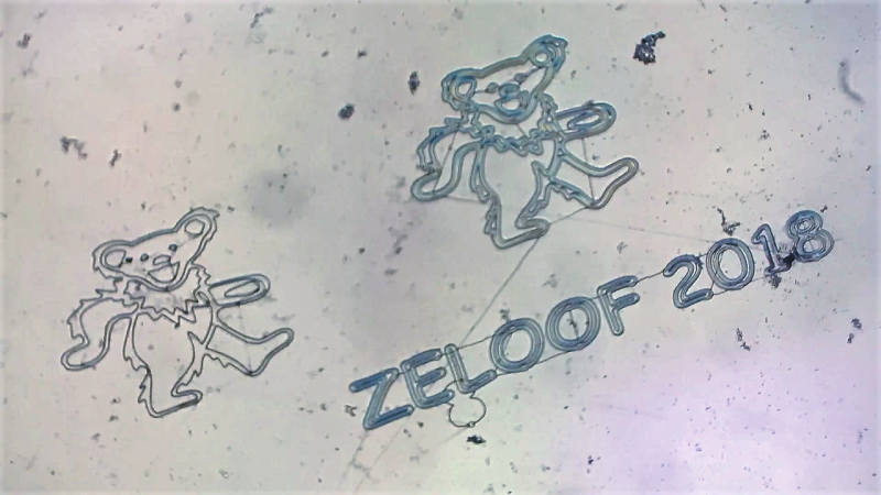
[Sam] is now looking into using the electron beam of his SEM as a sort of CNC laser engraver to produce much finer features. The process involves spin-coating silicon wafers with SU-8, an epoxy photoresist normally used with UV light but that also turns out to be sensitive to electron beams. He had to modify his SEM to control the X- and Y-axis deflection with a 12-bit DAC and provide a custom beam blanker. With a coated wafer in the vacuum chamber, standard laser engraving software generates the G-code to trace his test images on the resist. A very quick dip in acetone develops the exposed chip.
[Sam] says these first test images are not too dainty; the bears are about 2.5 mm high, and the line width is about 10 μm. His system is currently capable of resolving down to 100 nm, while commercial electron beam lithography can get down to 5 nm or so. He says that adding a Faraday cage to the setup might help him get there. Sounds like a project for Christmas break.


Similar, although a different substrate: http://www.cmarcelo.com/sandcastles/
GDTRFB ;)
Been going on for probably about as long as chips have been made.
http://www.writingfordesigners.com/wp-content/uploads/2015/04/microchip2.png
Maybe, but not by an 18-year old in his garage…
They grow up so fast.
Not undermining their work. Just pointing out that there are many, many examples out there to look at.
The real deal here is that he’s etching these with the beam from an SEM, and not just putting art in litho masks. (Which is also cool.)
<imghttps://micro.magnet.fsu.edu/creatures/images/russians.jpg
More:https://micro.magnet.fsu.edu/index.html
Is that pedobear?
This is like people who only think Mr. Potato Head came from Toy Story.
True, but you’ve got to realize that people come from all sorts of backgrounds. Hirudinea seems to have been raised by 4Chan rather than hippies. (Let the debate begin about which is worse!)
No, it’s the dancing bear from the Grateful Dead: https://liquidblue.com/music/grateful-dead/bears
I thought it looked like the logo of a former employer of mine, Bear Automotive.
It turns out the Grateful Dead may have cribbed it from them: http://www.roadarch.com/signs/bear.html
Thanks for the explination, I feel much better now.
Hello!
It was very interesting! What is software do you use? I can’t find LaserGRM v.1.0.1. If it possible, may be you gsen my arfive wich one?
oh, ok it’s LaserGRBL i find it.
I wonder if the guts from a CD/DVD burner could be used for something like this?