When a friend of [Tom Verbeure] came into possession of two HP 33120A 15 MHz function/arbitrary waveform generators, he could not resist giving them a try. Although not exactly high-end units, the HP 33120A makes for a pretty nice unit for a home lab. During the first test run, however, [Tom] discovered that one of the units had a dead output, which made it rather useless. Undeterred, [Tom] set to work diagnosing it, helped by the repair manual and full schematics.
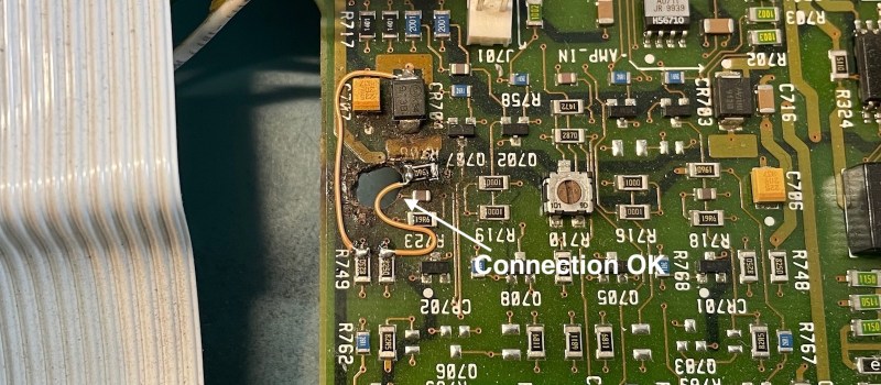
While the cause was quickly tracked down to the general area around an exploded MLCC, fixing the fried Zener diode that may have initiated the short on the -15V rail revealed an unpleasant surprise. To [Tom]’s horror, he saw a portal to Hell itself open when part of the PCB caught on fire due to an internal short. After making sure to capture a video of this event, he then proceeded to use a thermal camera to track down the hot spot and uses a drill to remove the short.
While one can argue with the use of a drill to remove shorts on inner layers of a PCB, ultimately the fix was effective. A look on the schematic and comparison with the functioning 33120A unit later, all it took was two bodge wires to restore functionality. After this event, [Tom]’s friend gave him the repaired unit as thanks, and definitely not because [Tom] had begun to refer to it as ‘his precious’.


Having done this: take a file to the hole after drilling. It’s really easy for a drill to wipe metal from a ground plane down to contact other traces or a power plane. If you use a fine file and go all around the outside, it removes material in fine enough bits that it’ll clean up the smeared metal without making the short worse.
A lot of the HP/agilent/keysight function generators from this era have a pretty straightforward output that also has a nice amplifier in it, and that amplifier’s kinda delicate so if you, say, attach it to a supply, you can cook the amp, but the function generator will still work at lower frequencies, like in the khz range.
That’s good advise!
In this repair, I didn’t add a missing decoupling cap yet, so when I open the unit back up, I’ll do some filing as well.
“Though not exactly a high end unit”? Maybe not (ok, certainly not) by today’s standard, but at the time, it was a premium unit for everything into the HF band, in particular with the ovenized crystal or external clock/sync option) The price was absolutely high end (for an AWG, not a frequency standard) when it was a current product. Still makes a decent showing against similarly priced new units.
Still a daily driver for me, with frequency at better than 1ppm with the base model crystal, and voltage at better than 0.01% over the range. Annual cal check with the last change of cal parameter maybe ten years ago when I bought my current unit.
I have a couple more modern units, but this is still my go to for most jobs where I don’t need multiple phase-synchronized signals (The two channel Rigol 20MHz can’t seem to hold phase sync more than about 180 days, implying that each channel has it’s own reference. The frequency is a bit more stable than the 33120A, though, on both channels, but with no better THD, and a more complex user interface for basic functions)
Drilling out shorts is not new. I was doing this kind of thing on old style PBX telephone systems in the 1980s. However, I did not use I.R. imagery to locate the mid layer shorts. Instead I used an in-house designed device we called a CPI, or current path indicator. It was a very sensitive differential opamp with coaxial test leads, capable of measuring a small voltage drop on the short length of a component lead. By injecting a low level current into the shorted circuit I could learn the direction the current was flowing. Once the short was located, I could drill out the PCB via where the short was located. Then epoxy the component back into place and rewire with 30 AWG Kynar.
In especially desperate situations, some people would use what we called a short buster. Essentially a capacitor bank that could blow open the short with a big current dump. The problem was this would leave a carbon track behind that eventually resulted in a circuit failure.
[relatively] Cheap IR cameras (FLIR) are a wonderful troubleshooting/diagnostic tool! When I first started doing designs, it took a desktop size box and a container of liquid nitrogen to see hotspots on a PCB!
Now it’s far better to ignore the FLIR lineup entirely and go for one of the far higher performance Infiray sensors instead. And they’re cheaper!
Where can I find these cheaper InfiRay sensors? The ones that I can find through Google are all more expensive.
We have a FLIR at the office, but it’s too easily fooled for troubleshooting. A cheap infrared thermometer works great. Held over a board and slowly moved, you can see follow the heat rise until the problem is localized. The smaller the sensor area, the better it works.
A sheet of “liquid crystal” film works well also when laid on a the solder side of a circuit board, but the IR thermometer is my go-to tool.
I agree completely, however my original work locating internal shorts was in the 1980s and the only cameras available then were FLIR cameras with a pure sapphire lens. Check out the pricing on those !
My precious…
“While one can argue with the use of a drill to remove shorts on inner layers of a PCB…”
Is there an alternative? I would be genuinely interested in hearing what the argument is.
Possibly something like remove connection to all the track concerned and rewire all on surface? It’s easier to control the short removal but the solution is just as messy…
I use a modified dental tool on which I made a chisel end to excavate through layers. Under a microscope, you can go slowly and remove burnt areas until the fault is cleared. The holes is filled with epoxy and any missing connections restored with “blue wires”.
Curious, if one spot of a multi-layer PCB has developed a short what’s the prognosis regarding more shorts appearing elsewhere on the PCB? Has it reached an age where the material has started breaking down?
Or is this just the result of a design where there is too much heat in that one spot and years of baking created a carbon path?
I had the same question. That’s why I will never sell this 33120A on eBay.
It’s possible mistreatment of the output stage overheated that specific area and caused the short. I have HP equipment that is a *lot* older than this, like germanium transistor stuff, that is still going strong, and I doubt it’s an inherent problem with the pcb inner layers that caused this.
It’s possible that this issue was due to mistreatment of the output, but in this case unlikely. I don’t know a whole lot about analog design, but the Zener diode seemed to generate a voltage rail was feeding power to the early stages of the amplifier.
It was probably just some one off defect that just happens when producing stuff at scale.
This is often a result of layer-to-layer registration of the artwork. IPC standards require a certain tolerance to be acceptable and sometimes there is an offset in the artwork, especially for large area PCBs. Imagine a transparency for each layer and all stacked together, some slight offsets are expected. If one layer is off by too much, there may indeed be several areas where the standard “keepout” zones are violated. For low voltage circuits, the keepout is typically no less than 8 mils. Check out this video https://vimeo.com/314566748 ~doug
I love how the video starts with…
“Euro Circuits TV
Presents
An Informative Video ”
Do they produce disinformation videos as well?
B^)
If you ask them, let me know.
“But that day is not this day!”
Years ago at a Repair Cafe I was tasked with repairing the power connector on a Toshiba laptop. The centre pin of the barrel jack had come loose in the PCB pad and the through-plating was shot, so I did what I’ve done many times before – I scraped off the soldermask and filleted solder across. I would have added wire or solder wick as reinforcement, but decided to test first. And their was a dead short across the power input – a short which I couldn’t find. One of the members of the hacker lab we were working at brought out a FLIR camera and pinpointed the short. I removed the connector and drilled, then soldered wires to appropriate points and applied power. And I had my own Eye of Sauron…
I took the computer home to work on it. I ended up with a rather large hole that I had carefully filed and sanded so the PCB was very thin at the inner edge and got thicker farther away from the hole, because the short was between internal layers. I literally “sanded for maximum resistance”; before I started using my ohmmeter I tried using the power brick, and Sauron reappeared…
When I was finally done I wired in a barrel connector pigtail style and left it hanging out the back of the computer – that was all I could do. Years later I learned that the power connector on that particular Toshiba was so problematic that even very experienced laptop technicians simply refused to attempt the repair. That made me feel a little better about the whole fiasco.