Repairing A Couple Of Very Expensive Registered DDR5 RAM Sticks

It’s definitely a sign of the times when repair shops get handed sticks of registered ECC DDR5 RAM by businesses to try and fix, rather than just tossing the defective ones and slotting in a fresh bunch. This is how [northwestrepair] ended up with two of these ECC RDIMMs, with a current market valuation of a rather nice budget car.
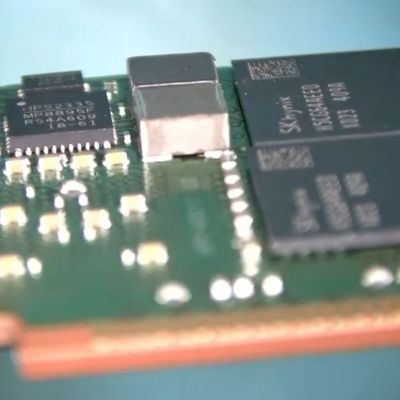
The 128 GB stick was first on the bench, with the fault being that it would fail DDR5 training on boot. This suggests that one or more of the DRAM BGA packages had developed a cracked solder joint, which is something that you could conceivably fix with more diagnosing and testing for a single IC reballing.

In this case doing a reflow cycle was enough to bring the RAM back to life, with the DDR5 training now passing without issues in a test system.

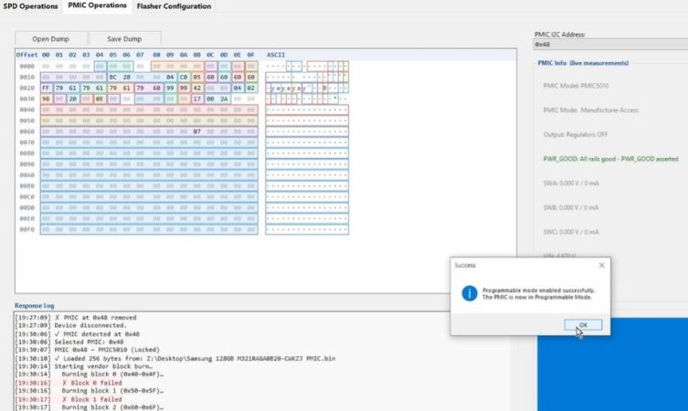
For the 256 GB stick things wouldn’t be so easy, as it seemed completely dead. This suggested a dead PMIC, as this is the component on DDR5 RAM responsible for ensuring that the DRAM ICs even power on. The SPD ROM was another option, so that got swapped first, which does require reprogramming the RDIMM. For this the earlier SPD dump image was reflashed, but swapping this chip made no difference.

After some additional reflowing of a few suspect ICs, still nothing happened. Following this a lot of reballing and other troubleshooting steps followed, only for the problem to be one shorted MLCC and a broken PMIC, potentially caused by whoever dropped said RDIMM onto the server room floor.

Cracked MLCCs do appear to be a very common cause of failures, as they’re often used as filter capacitors, same as for this RDIMM. Checking for shorts across a number of such MLCCs can be a good way to shorten a diagnostic cycle. Since this RDIMM was dropped, reballing every IC probably was still a good move as this may have cracked some solder balls.

Continue reading “Repairing A Couple Of Very Expensive Registered DDR5 RAM Sticks” →
A Headset Fit For A Hackaday Writer

I started writing this from a commuter train passing at speed through the outskirts of London, and my headset had just broken. The flexible joint that attaches one earpiece to the headband has snapped, leaving the earpiece dangling on its cable. This is annoying on its own, but what is annoying me enough to write about it is that this isn’t the first time. This is only the latest in a succession of headsets I’ve taken on the road with me has broken, not because of rough treatment, but simply due to flimsy or bad design. What on earth can I do about this?

Failure Built-In

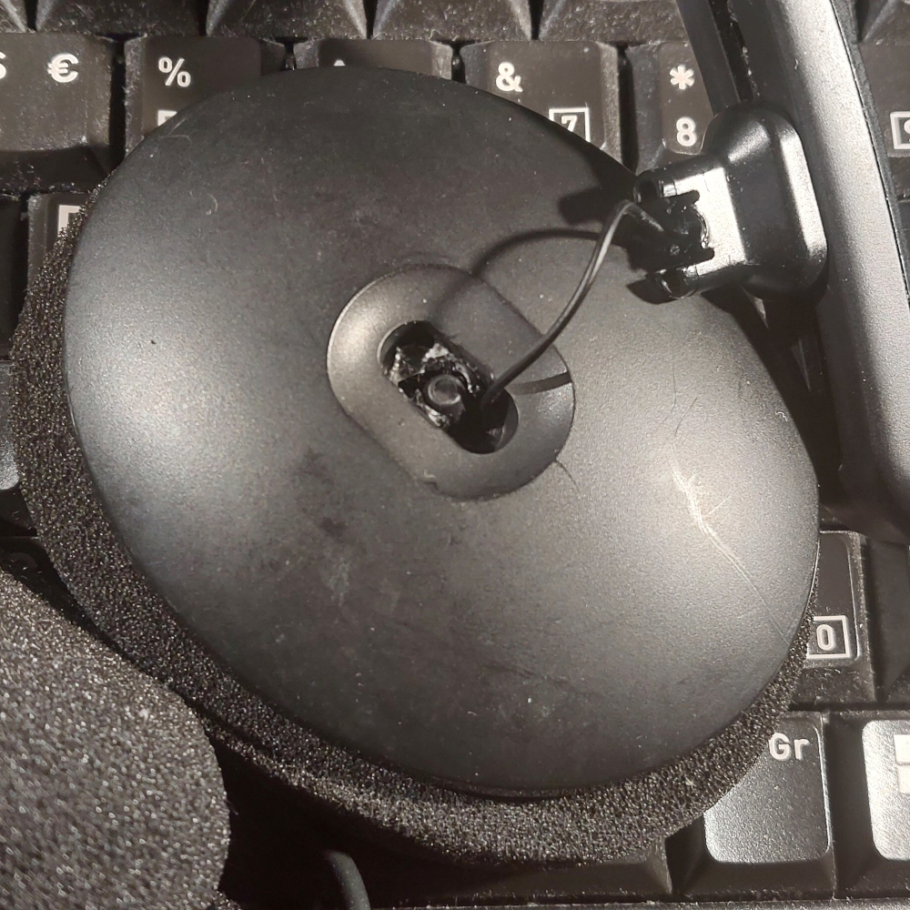
The earpiece of an EPOS headset, detached from its band.
Failure inevitable: the whole headset relied on a tiny piece of plastic in the centre.

The most recent three have been a JVC whose rotating joint allowing the earpiece to lie at a slight angle with my ear has failed, a quite expensive Logitech whose ear sponges failed closely followed by its USB cable, and now an EPOS whose ball joint has failed.

I repaired the JVC and got a bit more life out of it and I’ll have a go at repairing this EPOS, but that’s hardly the point. I’m paying not inconsequential money and I’m getting good sound quality and electronics, but I’m not getting anywhere near the mechanical quality I need. I could buy a set of tough DJ headphones such as the Sennheiser HD25, but they don’t come with a microphone, they’re not a headset.

So if I can’t buy a decent headset without spending military grade money on one from an F16 fighter, what can I do to make my own? I’m an engineer, damnit!

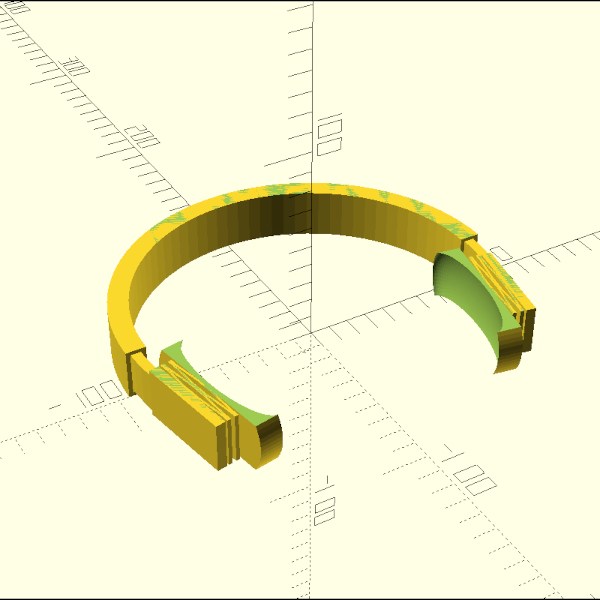
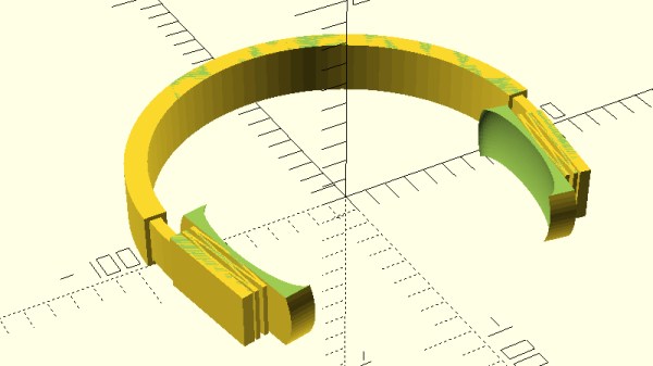
At its most basic, a headset is a springy band that goes over the head, with an earpiece at its end. But a human head is not a cube with vertical parallel sides, it’s a complex shape and every one is different. So those earpieces have to have some “give” in them in order to fit comfortably against the ear. In the simplest case this is achieved by giving the earpiece a soft surround that moulds itself to the ear, but most headsets incorporate some articulation. The earpiece must rotate a little around a vertical line parallel with the ear, and also with a horizontal line at right angles to the axis of the ear. The EPOS managed both axes by means of a ball joint, while the JVC had a stirrup with pins to achieve the horizontal motion, and a circular joint — the part which broke — for the vertical. In both case the weak point was a thin part of the plastic moulding which broke, on the EPOS a short stalk for the ball in the ball joint, and in the JVC a similar stalk for the circular joint. Any design I come up with must avoid this type of weak point, and spread the load of an earpiece over considerably more material than my broken headset. Continue reading “A Headset Fit For A Hackaday Writer” →

Tearing Down A Heavy Oscilloscope

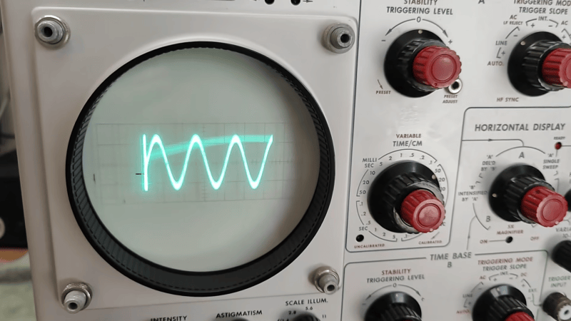
When [Thomas] showed his 1960s-era Tektronix 545A oscilloscope in a recent video, it made us both nostalgic and happy. Nostalgic because we miss the days when our oscilloscopes were “mainframes” that could take plug-in modules. Happy because we noticed the two handles on top to manage hauling the almost 70 pounds of tubes, transformers, and glass around if you didn’t have the requisite cart.

Not only did old scopes have plugins so you could reconfigure them, but there were also handy plugins and racks that could power them so you could build different test setups easily. This scope was an early version of that idea, but it only accepted a vertical section plugin. The mainframe part of the scope has 75 tubes, and the plugin, a type D, has six tubes, too. The power consumption was about 500 watts!

Continue reading “Tearing Down A Heavy Oscilloscope” →

The Game Boy Test Lab Provides A Cartridge-Sized Diagnostic Lab

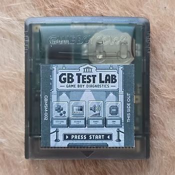
Most of the time when you see a repair video of a Game Boy it’ll be demonstrated with a cartridge inserted and booting up into the game, but does this actually mean that the system is truely fully functional? There can still be more intermittent faults, dodgy buttons, or even something like a defective link port — all of which can be much harder to detect than firing up a copy of Tetris. This is where the GB Test Lab cartridge by [Marcel Pflug] of the Game Boy Museum comes into play.

With the freely available ROM put on an EverDrive or similar flash cartridge, you can test a whole range of functions of the original Game Boy (DMG-01), most of them autonomously and some with some user input.

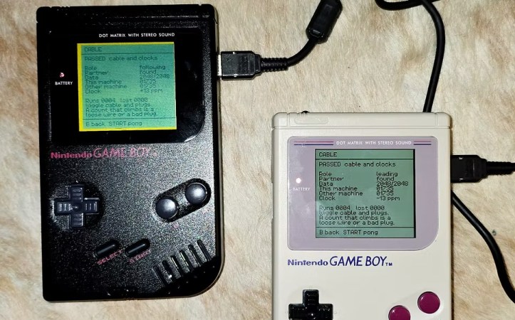
This is similar to the test cartridge that Nintendo themselves used in the form of the DMG-AGING-01, which validated the basic functionality of the handheld. Since then a myriad of test cartridges have been created by the homebrew community, but not all try to test quite literally everything possible. In the case of the GB Test Lab this includes the typical like CPU, RAM, interrupts, etc., but also key bounce time, intermittent connectivity and playing a game of Pong between two GBs connected by link cable as well as using the GB Printer.

Results are saved per GB and persisted if the flash cartridge has battery backup or similar. Overall it seems quite comprehensive and something that’s worth giving a shot if you’re the kind of person who owns one or more GBs. Perhaps the neatest part of this ROM is that it also contains a built-in reference for all the components and other useful details, including how to interpret results and symptoms.

Reviving The PoE++ Feature On A Ubiquiti Switch

Recently [The Parallel Port] was asked to take a look at repairing the PoE++ feature on a Ubiquiti switch that otherwise worked fine. This is a pretty nice 24-port rackmounted switch with 2.5 Gbit-capable RJ-45 ports and two 10 Gbit SFP+ ports, so by itself it’s pretty useful, but having the 400 Watt PoE feature just go AWOL still stings, especially if you bought it new for $800.

With power applied the switch starts up as normal, including its 1.3″ touch screen that provides direct port information as well as a fancy screensaver cum QR code for the AR feature.
After logging into the switch’s BusyBox console it showed that all ports reported bad for the PwrGood status, and there were PoE power status request errors in the log, but this could be just the consequence of something else. Using a PoE splitter it was confirmed that the PoE functionality was indeed dead.

After disassembly and some testing with a multimeter and thermal camera, a short and related hot spot on the PCB that the PoE power board connects to was identified, with the short persisting after removing this PCB from the switch. Since the switch had suffered a bit of an electrical event the TVS diode was checked, but it turned out to be fine.

Next to it, marked as fuses, were protective thyristor surge protection devices (Trisil), functioning as a crowbar device. These aren’t supposed to be shorted to ground until a surge event occurs, but these were indeed both shorted when measured directly. Clearly they had taken the brunt of the electrical event and sacrificed themselves in the process.

One replacement later of these devices the switch now happily reports a good PoE status and even was able to power a DC fan via the PoE splitter. Even if it wasn’t a particularly hard fix, this is definitely one of those cases where knowing how the protective circuit works can save a lot of time in diagnosing and fixing a fault.

Continue reading “Reviving The PoE++ Feature On A Ubiquiti Switch” →

Teardown And Repair Of An Insoma Water Timer

Water timers are nifty devices that can water the lawn at set times or keep that vegetable garden from turning into a dustbowl. When [electronupdate] timer refused to output water on any of its three outlets, he did the right thing. Instead of angrily checking the warranty on the sodding thing, he tore it apart to attempt a repair.
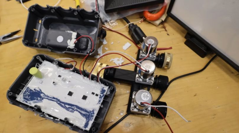
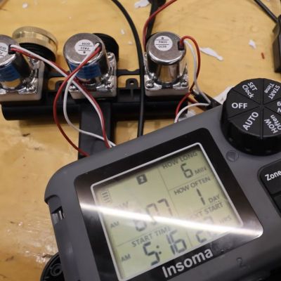
As expected, the design of these devices is quite straightforward. Three solenoids control whether an outlet is open or closed. A control board also handles the user controls and display.

There was no obvious sign of damage, and the PCB was potted in a white substance that should have kept out any moisture. A quick check with a battery revealed that the three solenoids also worked just fine, so the cause likely was somewhere on the — potted — PCB.

These solenoids are rated for 6VDC and take about 20 ms to act, but on an oscilloscope capture it was plain to see that the board was only putting out around 2V. This wasn’t enough to drive the solenoid, raising the question of what had gone wrong on the controller board and setting the stage for some fun epoxy potting compound scraping.

A good bit of elbow grease revealed the control ICs, the H-bridges that drive the solenoids, and the rest of the circuitry, including a power boost circuit with a big electrolytic capacitor. The latter had a bit of suspicious liquid near its base, which turned out to be the culprit. Perhaps the most annoying thing here is that this electrolytic capacitor had the temerity to fail after only four months of use, but at least it was an easy enough fix.

If we had been in there, we might have been tempted to avoid many future battery changes. Impractical, but we wonder if anyone ever built a water timer with a water clock?

Continue reading “Teardown And Repair Of An Insoma Water Timer” →

Reconstructing A Pin On A Pin Grid Array Package

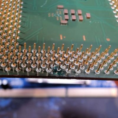
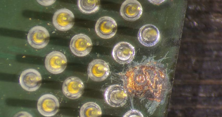
Before moving to land grid array (LGA) packaging whereby each pin on the substrate is just a copper pad, processors commonly used pin grid array (PGA) packaging, including the still highly relevant AMD AM4 socket. With PGA you get a pin soldered onto the copper pad which inserts into the ZIF socket, rather than a fragile pin on the mainboard side. Repairing a damaged PGA pin can be easy if just the pin broke off at the solder joint, or rough if the pad was destroyed, as in the case of this Pentium III CPU that [Bits und Bolts] recently tried to fix.

In the case of something like a ground pin or similarly unimportant pin you can ignore the damage, but in this case it concerned an important pin for this 1.2 GHz Tualatin PIII core, with the damage consisting of a well and truly destroyed pad. The first step to repair the damage is thus to try and rebuild the pad, which was done using solder mask and solder.

Although a PIII-era Celeron CPU is definitely not a high-value CPU, since they have so few and such large pins they do make for useful test subjects when it comes to PGA repair practicing. In this case the affected data pad and pin appears to have been repaired successfully, with it running overclocked to 1.6 GHz and crushing similarly or higher clocked Pentium 4 and AMD Athlon CPUs of the era.

Continue reading “Reconstructing A Pin On A Pin Grid Array Package” →