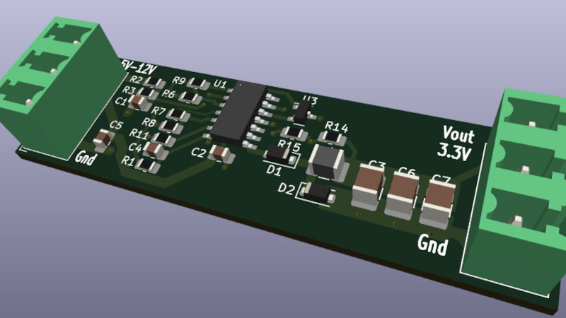
Switching regulators have delivered such convenience and efficiency compared to their linear siblings, that it’s now becoming rare to see an old-style three-terminal regulator. Modern designs have integrated to such an extent that for many of us the inner workings remain something of a mystery. It’s still possible to make switching regulators from first principles though, which is what [Aaron Lager] has done by designing a buck regulator from a quad op-amp IC,
It’s an entry in our Op Amp Challenge and it appears to be a work in progress, but the design is solid enough. We’re no fans of the schematic style of representing an op-amp chip as a rectangle rather than individual op-amps, but it’s simply a PWM generator with a final op-amp used as a driver for the usual diode-inductor-capacitor network. We’re guessing that the op-amp driver won’t make this the most powerful of switchers, but in this case that’s hardly the point. Build this if you’re interested in taking an op-amp out of its normal sphere, or if you’re interested in the workings of a buck converter.
Need more in the way of switching regulators from first principles? We’ve got you covered, with the ultimate regulator kit of parts, the Fairchild UA723.


I’m not sure those flyback diodes are required. The op amp would have a puh pull output, allowing for a low performance synchronous converter.
If you’re going to dispense with the diodes, then you can get rid of the inductor too, because it’s not doing anything. Then you can get rid of the oscillator and triangle wave generator as well.
It would certainly end up quieter, with less ripple. Heck, probably even has higher output power too.
I’d wager it’s even more efficient, at least going from 5 to 3.3V.
without the diodes it’s the same topology as a synchronous buck
…with an op-amp output stage in the place of switches. Good luck. Let us know how it works out for you.
It has pseudo push-pull output. As per the datasheet, drive power is Vs* Iout, and power dissipated in the load is Vo*Iout.
In this case without the diodes, it would operate like a linear regulator with bang-bang control smoothed through the inductor, making the most of the circuit a waste of time and super poor efficiency, like @Paul mentioned.
This op amp just isn’t designed to operate low impedance loads. Trying to run it open loop into a heavy load is going to be just horrible for recovery time and control bandwidth. Using the pwm to pull down a p-FET instead of driving through the top diode would be a major improvement, but would require inverting the polarity somewhere. Going to a boost cap/diode and running a n-fet would be even better. Replace the oscillator with a 555 like circuit, and use the 4th op-amp to do synchronous rectification would be the next step
From R14, R15 in the schematic, it looks like it’s going to try to make 6.7 volts on the output.
…assuming the 2.5V reference annotation is correct… which it isn’t.
The Max6101 is a 1.25V reference, which makes this work.
Oh yeah. I’ve built several of these. Two of them are in my 5FP7 supplies for the tube and the deflection circuits.
For just a buck?
I’ll buy a dozen!
For a basic circuit, you can steal some ideas from the MC34063A.
You’d have an input capacitor, P MOSFET power switch, a flyback diode, inductor and output cap.
You’d have an output voltage compared against a reference voltage – 1 op amp used as a comparator.
You could use a fixed frequency (an oscillator – 1 opamp) to enable the MOSFET, then turn off the MOSFET either at the off time of the fixed frequency, OR when the peak current through the inductor exceeds a limit (another op amp used as a comparator.) This would give you PWM regulation with a peak current inner loop and output voltage outer control loop.