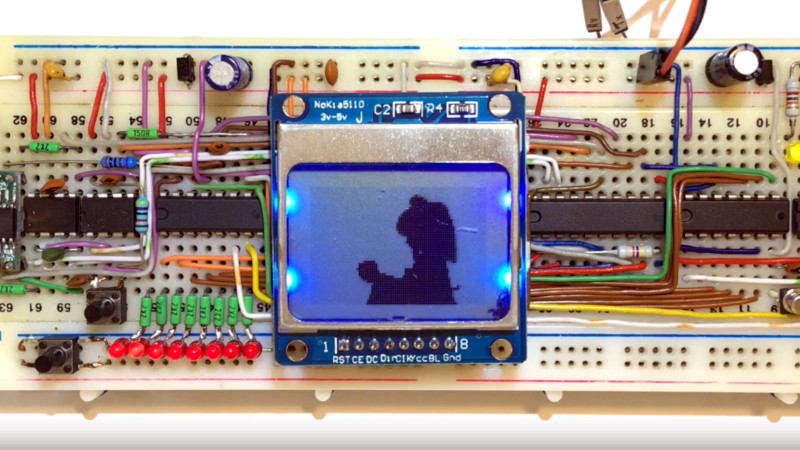
We’re no stranger to homemade CPUs on these pages, but we think that [Jiri Stepanovsky]’s 16-bit serial CPU might be a little special. Why? It has an astonishingly low chip count, with only 8 ICs in total. How on earth does he do it?
While a traditional TTL CPU has a relatively high chip count due to a parallel data bus, registers, and discrete ALU, this one takes a few shortcuts by opting for a one-bit serial bus with serial memory chips and an EPROM serving as a look-up-table ALU. Perhaps the most interesting result of this architecture is that it also allows the CPU to dispense with registers, like the Texas Instruments 16-bit chips back in the day. They all live in memory. You can see it below the break in action, streaming a video to a Nokia-style LCD.
Such a CPU would indeed have been unlikely to have been made back in the day due to the prohibitive cost of buying and programming such a large EPROM. However, old computers like the EDSAC also used a serial data path and mercury delay line memory to manage complexity. But for a solid-state CPU in 2023, we think the design is innovative. We think it would be challenging to reduce the chip count further — and no, we’re not counting designs that use a microcontroller to replicate a block of circuitry; that’s cheating — but we’re sure that somewhere there’s a designer with ideas for slimming the design further.
Thanks to [Ken Boak] for the tip.


Put it in an FPGA.
These devices all *do* use the simplest form of programmable logic: an EEPROM.
They also don’t translate to “simple” in an FPGA: 768 kB of program space, for instance, would take up a *lot* of a small-ish FPGA.
Most FPGAs require an external serial flash chip to hold the bitstream that configures it. Once booted then any extra space on the flash can be used to hold the program data. Your 768kB of video data wouldn’t make much of a dent in a typical 16 or 32Mbit flash chip.
The other thing to remember is that they are doing something very similar to the EPROM, but many times over and on a smaller scale. The basic unit of the FPGA is a LUT, which is a small memory cell with typically 4 inputs and one output. What you have is a 16 x 1 bit memory cell programmed by the bitstream on startup. Multiply that by a few thousand times and add custom function blocks (for things like RAM, IO and routing) and you have an FPGA. Even a small FPGA should be able to implement this design, but not by storing all the logic terms in a single large Look Up Table that the EPROM effectively is.
You can’t just look at bit capacity. SPI flash chips take a significant amount of logic to use them in anything other than a straight stream: the boot process for an FPGA is easy, you just clock out a fixed sequence and watch for the data to start arriving, and then keep clocking. No logic needed: it’s a fixed ROM, a shift register and a match.
But using them as random access is a lot different. It’s not hard to use them to, for instance, page ROM in, but in many cases this means you’d be better off with a denser instruction coding and having *everything* in a block RAM straight from the start.
Plus obviously you have to ask about bandwidth per cycle, access granularity needed, etc.
There’s a RISC-V serial CPU which operates out of SPI flash using XIP mode, which I’ve tried out, but it’s definitely not as small as I would’ve thought. A lot of it is just because of the overhead of implementing the interface.
Ah yes and as we all know video frames are infamously nonsequential in their access pattern. :P
RISC V is a 32 bit parallel core. This is a 1 bit wide serial core set to work on 16 bit blocks. Because of this SPI memory access becomes much simpler as there is no need to serialise/deserialise the data, you only need a simple state machine to set up an address then clock the data in or out. The video data it is working on is serial in nature, plus the display module is also SPI (probably sharing a lot of the logic) so I’m not sure where you get the idea of huge complexity from.
“RISC V is a 32 bit parallel core. ”
RISC-V is an *instruction set*. The core in question is SERV, which is a *serial* implementation of RISC-V: meaning it also operates only 1 bit at a time. It’s not a 1-bit CPU, it’s a 16-bit CPU with a serial implementation. This is described in the link.
“you only need a simple state machine to set up an address then clock the data in or out.”
Why yes, that’s correct! Oh, and guess what? A simple state machine is *not that different than a CPU in the first place*.
I mean, I usually *use* a tiny CPU to access the SPI flash, because hey, now I can program in *writing* to it as well, which is *much* more complicated.
SERV on an FPGA takes a grand total of 125 LUTs/164 FFs. An SPI flash core is probably within a factor of 2-3 smaller than that.
“so I’m not sure where you get the idea of huge complexity from.”
Huge is relative. Of course you *can* implement this in an FPGA with an SPI flash for the program ROM. It’s definitely a cool project.
But for instance: the “1-bit ALU + state machine” control flow? In an FPGA, that optimization is “use block RAM to implement logic,” and you’d *never* do it for something like this, because it’s an incredibly inefficient use of block RAM for this purpose: that 128 kB EEPROM is already the equivalent of 1 *million* flipflops! (And that’s *separate* from the program ROM).
Again, to repeat: it’s a cool project. Understanding that you can use memory as programmable logic is really useful! It’s the earliest trick people used to generate programmable logic!
But you wouldn’t want to implement it in an FPGA, because it’s not designed for it, so it doesn’t map well to it. Again, see designs like SERV.
Point taken about the serial RISC-V core. Once you have a Turing complete core you can run any instruction set you like on it (maybe very slowly and via software emulation, but it can be done).
The point I was trying to make is that, in implementing this in an FPGA, you wouldn’t try to write the whole look-up table from the original into BRAM, but rather extract out smaller terms and implement them in groups of or single LUTs. There will be many unused or don’t care terms in that ROM.
The RISC-V core you are talking about is small enough to fit on CPLDs, never mind an FPGA. If you can do that then this core should be possible to implement in a small (say 1K LUT, which is about as small as they get) FPGA. There are things that this design does that are trivial in an FPGA, for example using a 128KB look up table in the flash ROM to reverse the bit order of bytes coming from the RAM chips). Put another way, you wouldn’t do a direct clone of this design to have it work in an FPGA, but you should still be able to fit the functionality in a pretty small device.
Having CPU cores implemented as part of logic designs in order to achieve things that are possible, but much more complex in pure logic is pretty standard practice (many disc controllers contain ARM cores for example, and a standard of-the-shelf soft core is an expected part of any FPGA IP catalog). It is always a trade-off between time, complexity and speed.
“The point I was trying to make is that, in implementing this in an FPGA, you wouldn’t try to write the whole look-up table from the original into BRAM, but rather extract out smaller terms and implement them in groups of or single LUTs. There will be many unused or don’t care terms in that ROM.”
In other words… you’d make a completely different architecture.
Again: this CPU consists of a 128 kB memory used as a state machine/ALU, a 1 MB SPI flash, and 2x 128 kB serial SRAM chips used as CPU registers, program counters, flags, stack pointers and value, etc.
The entire *point* of this design is to just throw memory at things because memory chips are cheap. 128 kB of the flash chip is used as a lookup table to reverse bits!
Like I said, this is a study in using memory as programmable logic. Which is a super-cool thing to study. It is not a study in building a soft CPU for an FPGA, which is an entirely different optimization problem.
I think you’re confusing architecture with implementation. You can still have the 17 bit input, 8 bit output style decoding in the FPGA, but the implementation of that would be considerably different. Architecturally the two machines could look the same (same logic steps, inputs and outputs) but how you choose to implement them would have to change if nothing else because one is EPROM based and the other is programmable logic.
No, I’m really not. There are tons of *architecture* details here that are influenced by the fact that it’s memory rich and logic/FF poor.
Just look at the instruction set, and read the article. All the moves and arithmetic and logic instructions operate over the full 64k space, because to this CPU, registers and memory are the same thing.
In other words, it’s flat out *built* on the assumption that you’ve got that memory space for free. There are two sets of load/stores because of the second RAM so it can be used as a stack cheaply.
In addition, the opcodes aren’t optimized for logic since they’re controlling a memory and the organization of that memory is arbitrary. You get stuff like SUBI/SBCI being 0x1F/0x20 (bottom 5 bits different) even though they only differ in whether or not you blank the carry or not (so they really should only differ by 1 bit).
I really could go on and on. Again – let me be clear, this isn’t a criticism of this project or of the architecture! It’s absolutely not. But the only reason you’d implement something like this in an FPGA is if you had the serial RAMs and EEPROM already on the board as well.
Having registers in RAM isn’t a new idea (see the TMS9900 series for an example), and you don’t need the full amount of RAM to implement the architecture. It’s an implementation decision whether or not to use the remaining BRAM, use a bigger FPGA or connect up an external RAM module (or modules). The fact that an architecture is designed with assumptions about the hardware it will run on doesn’t constrain it to that hardware, nor does implementing it on a different set of hardware make it a different architecture.
As you yourself stated, a RISC-V core can be implemented in a serial machine. This does not disqualify it as a RISC-V core. Architecture and implementation are two different sides of a coin, and it it possible to implement an architecture in many different ways while remaining true to the design.
“Having registers in RAM isn’t a new idea”
I never said it was! I seriously have no idea what you’re even trying to comment on here anymore.
My comments were about *this* architecture and *this* design. Yes, of course, you can design a serial CPU in an FPGA. I’ve already directly mentioned one. Yes, of course, you could design this architecture in an FPGA. I’ve also already said that.
What I’m saying is that *this* design is not well suited for being implemented fully in an FPGA, because it’s designed around the fact that memory is cheap and plentiful, and this is not true relative to logic in an FPGA.
I don’t understand why this is remotely controversial. This isn’t an efficient way to build a CPU in an FPGA. It’s a really neat way to build up a CPU out of memory chips. FPGAs don’t have serial RAM onboard, and while they do often have SPI ROMs, you’d be much better off implementing either an SPIx2 or SPIx4 interface for it, which doesn’t really take a lot more work. Or even XIP.
“and you don’t need the full amount of RAM to implement the architecture.”
No, of course not, but without the full 64k x2 space it’d be a poor design choice, because you’d be wasting large amounts of instruction space since all the instructions have a full 16-bit address space in their encodings.
Again – could you do it in an FPGA? Sure. Is there a reason to (other than curiosity)? Not really. It wouldn’t compare favorably in terms of size or speed to other architectures.
This isn’t a criticism of the design. I’m just saying you’d be trying to fit a square peg in a round hole. Sure, you can *do* it, by hacking the square peg into a round hole. But you could also just… find a round peg.
You’ve been spending your time trying to tell me that the architecture would have to change if it was in an FPGA (it wouldn’t, only the implementation), that it would be a waste if you didn’t have 64K of RAM because all the arithmetic ops are designed to work with a 16 bit address space (so what? Most 8 bit microprocessors have a 16 bit address space and no one complained if they came with less RAM than that). BTW code runs from the flash ROM, so code size is limited by that, not the RAM. You say it wouldn’t fit in a small FPGA (not only would it fit, but it seems that there are FPGAs on the market that would do pretty much everything without the need for external chips – for example the GOWIN GW1NS-2, which is flash based (no need for an external config ROM) and has 32Mbits of PSRAM in addition to 72Kbits of BRAM and 2K of LUTs), that there’s no point (other than the challenge) of doing it (erm, that’s the reason for most stuff around here, and many FPGA cores in general).
Put simply, you’re trying to convince me that it can’t be done, and if it were done it would work poorly, would be wildly inefficient and wouldn’t be practical. In case you hadn’t noticed the original is slow, inefficient and not very practical either. The argument is purely whether or not this could be done in a small FPGA with fewer chips, to which my contention is that it could (and probably considerably faster).
CPLDs however, almost always have nonvolatile memory onboard.
Some FPGAs are also flash based (the Intel MAX 10 for example), but you’re still going to need external storage for the code/data (the design has 8Mbits of flash ROM), which is kind of expensive to get in an FPGA (and outside CPLD capacity completely).
I’m… trying to convince you it can’t be done by saying, explicitly, that of course it can be done?
And no, I never said it wouldn’t work as efficiently either. I said it wouldn’t be an efficient *use of resources* in an FPGA because it trades logic for memory.
Why ruin it? 😨
The beauty on such things lies in the use of an [E]EPROM as an address-decoder/mapper/etc ..
If it was done in an FPGA, it wouldn’t be fascinating and inspiring, at all, wouldn’t it? 😔
“Put it in an FPGA.” a typical comment from someone who has no idea about the concepts of minimalist hardware.
Had you said “Shove it up your ass” I might have been more impressed by your dimmissive viewpoint of a neat hardware design,
A five word response hardly illustrates your position of hardware superiority.
Sorry about being dismissive. https://bit.ly/WhoIsSteveCasselman
Many of you should check out hotwright.com. I’ve developed an advanced runtime loadable microcoded algorithmic state machine. You program it in a subset of C and can use gdb to debug it. The size of the machine expands to match your code. A small program generates a small machine. The Hotstate machine can be used to make controllers or CPUs as well as what I call a NoISA processor. It’s all portable to any FPGA tools that support SystemVerilog. I publish all the hardware code so you can simulate and port this anywhere.
That’s what I was going to suggest!
CPLD
This architecture could definitely be designed in an FPGA. The 128kB EPROM contains a lot of repeating logic, which could be eliminated together with the rest of the 74HC logic, and implemented in an FPGA. It would probably even run faster.
However, I believe you kinda missed the point of the project.
It is centered around the most simplistic programmable circuits -> memories, and what they are capable of. The whole architecture is designed around them.
Implementing a soft-core CPU inside an FPGA is a completely different thing. There is a lot of awesome soft-core CPUs out there, with architectures designed specifically for them.
This project is not trying to replicate them:)
If there is a award so supreme cleverness, this state-machine CPU, and it’s designer should get it.
Can I use a Z80 to reduce the chip count of a CPU? Z80 is no microcontroller :)
But seriously, this is a seriously bad serial apple! I was a bit surprised by the low audio quality at first, but apparently it plays the audio itself too, and that makes it even more impressive.
Cool! But how did it work even there is no power provided to the breadboard?
There is a 2 pin power cable on the power rails. The sound however is done on a secondary board, as mentioned in his video description (and video/sound are recorded separately for performance reasons).
True, but what I see in the video is the other end of those two pins are hanging in the air? That’s why I’m asking
The shadow looks like it’s 2 spare connectors from a 4-wire cable, I guess to power a second breadboard.
Exactly. It is an 4-wire UART cable -> 2 power lines + 2 data lines, which are only used for programming.
?
You could use one FPGA and one EEPROM if that is withing the rules.
You will need multiple power regulators 5,v 2.x and 1.x .
C-H Ting Lattice 1802 FGPA hardware/interactive software OS solution?
https://www.google.com/search?q=c-h+ting+fpga+1802+fig+forth&oq=&aqs=chrome.0.35i39i362l4j46i39i199i362i465j35i39i362l3.219637j1j7&sourceid=chrome&ie=UTF-8
What makes this a CPU? Where do all the calculations and conditional jumps happen? Isn’t this thing just a serial data player?
All of the arithmetic and logic functions, including jumps, are happening in the state machine in the eprom (that is unfortunately behind the lcd and blocked from view) and two latch chips.
This form of state machine is a textbook example of a pure turing machine.
It looks like they are using 7 bits to store state and 1 bit as a data bus to drive a 74’595 latch, which is performing all of the memory read/write operations including the instruction fetch/execute steps.
The LCD is in the schematic as a memory IO mapped device. Not sure about the sound.
The sound is created via a memory mapped shift register (74HC595) with its 8 outputs connected to a R-2R DAC.
Unfortunately, it occupies the same address lines as the LCD, so the CPU can either drive display or play audio, not both. To be fair, it is also too slow to do both:)
Should you have sufficient attention span to visit the website – you can see the full ISA.
Try to assimilate all the available information first – before you start firing blanks into the dark void.
“Isn’t this thing just a serial data player?”
Doesn’t need anything more to be Turing Complete.
I remember back in 1975, a member of our computer club (i think his name was Gary, he was a senior at Case Western Reserve) built a 16 chip ttl cpu. I think it had a 74181 alu. So this is not new. Ok it was only 8-bit.
This doesn’t even have that… its much simpler than even a bitslice CPU like you are talking about.
There was a time before the microprocessor when ALL CPUs were built from 74 series logic or equivalents. There was even a time when processors built from 74 series were faster and more powerful than microprocessors (workstations like the 3 Rivers/ICL PERQ or the Xerox Alto were 32 bit machines before microprocessors had made it to 16 bit). What is remarkable is the low chip count.
Jenny – thanks for posting. George needs a lot wider exposure here.
There may be some naysayers – but I guess they know Jack s**t about how bit-serial actually works,
To Educate, Inform and Entertain – can you tell that I am ex-BBC
See you in HB next weekend?
Indeed, if you don’t understand it read the website :)
And yes.
Why is it always f**king Bad Apple?
Have you never owned one? Me neither!
It’s not just a bad apple.
There is also that picture of a naughty looking young girl with a hat that is trying to get her history erased now she is all old and wrinkly.
And some other times it can also be playing doom or emulating a 555.
It is a reasonably short monochromatic video which is used widely enough, that the projects can be compared/”benchmarked” between each other.
For the same reason, so many systems can play DOOM,
and so many machine learning systems train on MNIST database.
haha i wish i’d invented it
This is one of the most interesting CPU designs I’ve seen in a long time. Amazing work.
I wonder if you could eliminate the microcontroller needed for programming by bit banging the serial flash protocol using the modem lines on a serial port.
So in essence a bunch of large look up tables that operate on themselves? Me love! <3
And there’s me trying to figure out what I could use this design for in my projects.
It would be nice to see this implemented as eityher a hybrid module or even put on a single, custom chip, just to see it done.
the funny thing is that as custom silicon, the big ROM look up table would actually take more chip real estate than other designs that seem more complicated when implemented with discrete logic
Yeah, that’s the problem with using a single ROM lookup table for logic. It was done back when no one had any other choice, not because it’s a good idea at the silicon level.
It’s incredibly inefficient because you inherently need all possible combinations of the inputs – you’re creating a 17-bit logic function, and the truth table for that logic is incredibly sparse/repetitive, so you’d be better off factoring it into smaller intermediate chunks. Which is exactly the way FPGAs work.
For instance, if you want to use memory to implement 2 separate 4-input, 1 output LUTs (fundamentally 32 bits of data), you need a 256×2 memory (fundamentally 512 bits of data), meaning you end up duplicating things 16-fold.
FPGAs actually have optimizations for using internal memory as logic terms when logic becomes scarce, but it’s very rare for it to actually be useful.
Wow – what a wonderful thing. Congrats and thanks.
Another similar design is http://mynor.org/ – there’s an explicit single NOR gate used as an ALU, instead of a LUT in ROM, – otherwise it’s more or less the same. And it runs Forth!
Forth you say? Daring. :-)
Fun project!
The detractors all have their valid points but hey, give this guy a break as he has made something quite ingenious. Well done I say!
But can it run Doom?
Thank you very much for posting, Jenny.
It is great to see the feedback and discussions it leads to.
Thank you:)
All the champions of minimal processors do the same trick: hide logic in memory. But nevertheless, it is good that young people are delving into the depths of computer calculations. Well done.