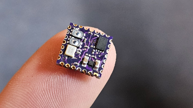
Is [William Herr]’s RPDot actually the world’s smallest RP2040 dev board? We can’t say for sure, but at 10 mm on a side, we’d say it has a pretty good shot at the record.
Not that it really matters, mind you — the technical feat of building a fully functional dev board that’s only 3 mm longer on each side than the main chip is the kind of stuff we love to see. [William] says he took inspiration from the [SolderParty] RP2040 Stamp, which at one inch (25.4 mm) on a side is gigantic compared to the RPDot. Getting the RP2040 and all the support components, which include an 8MB QSPI Flash chip, a 3V3 LDO, a handful of 0201 passives, and even a pair of pushbuttons, required quite a lot of design tweaking. He started his PCB design as a four-layer board; while six layers would have made things easier, the budget wouldn’t allow such extravagance for a prototype. Still, he somehow managed to stuff everything in the allotted space and send the designs off — only to get back defective boards.
After reordering from a different vendor, the real fun began. Most of the components went on the front side of the board and were reflowed using a hot plate. The RP2040 itself needed to go on the back side, which required gentle hot air reflow so as not to disrupt the other side of the board. The results look pretty good, although those castellated edges look a little worse for the wear. Still, for someone who only ever worked with 0402 components before, it’s pretty impressive.
[William] says he’s going to open-source the designs as well as make some available for sale. We’ll be looking out for those and other developments, but for now, it’s just pretty cool to see such SMD heroics.


Impressively compact.
However, I see the castellated edges as a way to connect the ‘difficult’ parts of a design onto a cheap, low-tech pcb that connects external project-specific parts like leds and connectors. As such, the board wants to lie flat on the bigger board with the castellations soldered to it. Having components on both sides makes this difficult unless that bigger board has a carefully-shaped hole in it to give clearance.
I’m reminded of BPI-RK3588-LGA, except here you don’t even get enough overlapping width.
Agree, the double-sided assembly directly defeats the purpose of castellated edge pads.
But still, very cool proof-of-concept! All the more props for manual soldering it all.
Good job!
If it’s standard pitch, you could make a “socket” out of pin headers.
..which also wouldn’t benefit at all from the castellated connections.
missed opportunity to make it be PLCC32 then (1.27mm pitch)
exactly. poor man’s 3d board architecture. if you lift it up a bit you can get parts on the board under it. so you’d have 4 layers of components in the space.
There was a PCB construction method once used that used a stack of PCBs connected by wires along their edges. Some called this “cordwood” construction.
Not at all. All you need to do is put a square hole in the PCB. Its not a big deal at all.
Positing at risk of spamming… But I’m working on exactly what you’re talking about
https://hackaday.io/project/192207-crapi2040
Still tiny, but still useable with USB!
Defo would not use this product due to components being on both sides. Dont bother taking it to market IMO.
I’ve used this board though: https://thepihut.com/products/tinypico-nano which is awesome. Great design. 100x user friendly. Still a small footprint.
I would simply revert the castellations to normal holes. It doesn’t get much bigger (still consumes the same hole pattern on a matrix board) but can be mounted on pin headers.
Useless
The idea here was how small he could get the circuit. How do you feel about things like clown cars or the bible written on the head of a pin??
Your comment does a better job of expressing “useless”. If you don’t like it just move on. I dont personally see a use for this but….
1. did they make it for a reason…yes.
2. did they learn something…. yes.
3. Does it fit exactly what they wanted? Maybe, maybe not. They can now refine their idea and are that much closer to getting exactly what they want.
4. Did they share their ideas and experience with this great community… yes. I very much appreciate that they took the time to get all this together and share it.
They are adding to and growing the community.
Your trolling is subtracting.
What is the saying. If you don’t have anything nice to say, don’t say anything at all.
Your comment is not even constructive criticism
Raidcore, I agree with you! Very well said!
Very, very nice work! Like a poem, it takes me back, yet forward.
Maybe make it fit in a PLCC socket or something? Neat project, and a good exercise in compacting and space saving but the trouble of integrating it in a board isn’t much different I think than dealing with the raw RP2040, regulators and memory, to be completely honest. But take that same skill and care and put it into designing an entire project / product and things will be compact and awesome (not that this isn’t compact and awesome)
Now, if you’re trying to hide it somewhere for something nefarious, like inside a keyboard, then yeah it’s great as-is.
The best use of this would be for one of those miniatures where you solder enamel wires to the edges and stuff it inside a toy car.
heh everyone else already pointed out the dubious utility of castellated connections on a double-sided board but i want to add that i personally don’t see the point of an rp2040 without a usb port! it seems to me like anyone who is ‘productizing it’ in such a fashion that they care this much about space and don’t need the convenience of a usb port will probably be happy to just use the naked chip in their custom pcb design.
but! it’s definitely a hack!
Sadly there are too many inside the box thinkers that made those comments. All one would need to do is open a square hole in the PCB to mount it. If they want USB they can put it where they need it on their main PCB. It gives the user more flexibility the way he designed it VS slapping a USB connector on it.
That is how I too saw how to use this board. Design a ‘your’ PCB around this one with a square hole to accommodate it . This board (as I see it) wasn’t designed to just ‘plug’ into your PC ;) . Similar to the stamp, and other designs.
If only they’d just manufacture the RP2040 in SOIC (1.27mm pitch), TSSOP (0.65mm) or QFP (with the exposed outward pointing legs)(0.8mm). That way anyone with a steady hand and a pointy iron could solder it to custom PCBs, no need for carrier boards. QFN not only needs paste soldering, which many of us can do, but is particularly tricky to paste solder and hard to debug, no way to make an ohm measurement from the pin itself to the trace’s pad. Exposed leads would be so welcome!
Or something like the o’ 68332 CPU package where you just pressed the CPU into a socket that was soldered to PCB. We used those a lot back when. No soldering of the CPU needed. Sure a bigger foot print, but so what…. Easier for the do-it-yourself people to design around :) .
DIY people value a form factor which is smaller than the Pi Pico board, but big enough to be hand soldered under a microscope or paste soldered with lower end equipment. Anything involving a special socket becomes so big you might as well use a full Pi Pico board, yet the QFN has horrible underside pads. The sweet spot therefore is SOIC/TSSOP/QFP.
There aren’t many ICs destined for more hobbyist applications than a raspberry pi microcontroller, but for whatever reason they chose to use this package. Probably because it doesn’t waste space and provides the maximum flexibility for breakouts of whatever format.
It doesn’t make a lot of sense to produce only an easy-to-use package. If that’s the case they’d probably still be DIP. Better to have a flexible package than a low-tech one
It’s easy enough to make it work the way you want. If you want probe-able pins, just make the pads longer so you can probe them outside the footprint. Of course, most of these carriers bring all the pins to the edge anyway so are easy to probe.
I’ve been working on a tiny RP2040 devboard too, but I’ve really really focused on usability…
https://hackaday.io/project/192207-crapi2040
Still just 1 square inch but bread-boardable and still breaks out every pin on the RP2040. Needed to get my hands dirty with 0201 components but it’s totally been worth it!
oh, and it has a USB port “built in!” :D
“SMD prototyping grid” :O
i see something new every day thanks
What if you used a dual sided flex PCB instead? Instead of the castellated holes you could bring out the connections to one side and plug your PCB into an FFC-connector. It has the added advantage that the module is replaceable. Maybe dual side tape might be needed to avoid it from “flapping” too much.
Have you tried this approach? I tested USB-C footprint on a board and it is “flapping”, but useful for power. I am wondering if getting out SWD & UART could be achieved that way. Also do you have suitable FFC in mind, which could contact well with Edge Connectors on board by by jlc/pcbway or similar?
But can you run Windows11 on it?