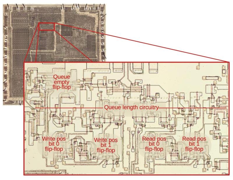
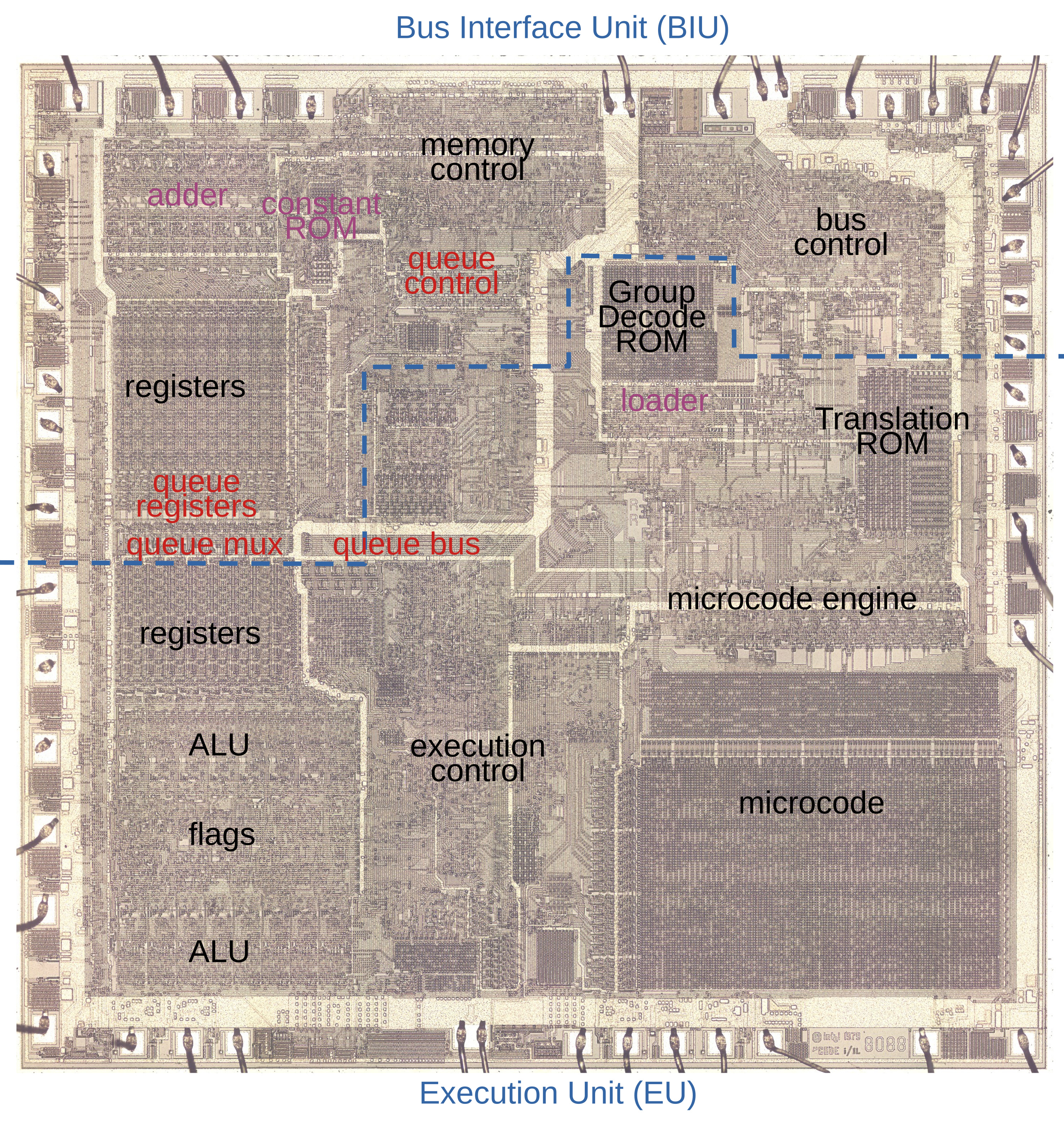
Cache prefetching is what allows processors to have data and/or instructions ready for use in a fast local cache rather than having to wait for a fetch request to trickle through to system RAM and back again. The Intel 8088 (and its big brother 8086) processor was among the first microprocessors to implement (instruction) prefetching in hardware, which [Ken Shirriff] has analyzed based on die images of this famous processor. This follows last year’s deep-dive into the 8086’s prefetching hardware, with (unsurprisingly) many similarities between these two microprocessors, as well as a few differences that are mostly due to the 8088’s cut-down 8-bit data bus.
While the 8086 has 3 16-bit slots in the instruction prefetcher the 8088 gets 4 slots, each 8-bit. The prefetching hardware is part of the Bus Interface Unit (BIU), which effectively decouples the actual processor (Execution Unit, or EU) from the system RAM. While previous MPUs would be fully deterministic, with instructions being loaded from RAM and subsequently executed, the 8086 and 8088’s prefetching meant that such assumptions no longer were true. The added features in the BIU also meant that the instruction pointer (IP) and related registers moved to the BIU, while the ringbuffer logic around the queue had to somehow keep the queueing and pointer offsets into RAM working correctly.
Even though these days CPUs have much more complicated, multi-level caches that are measured in kilobytes and megabytes, it’s fascinating to see where it all began, with just a few bytes and relatively straight-forward hardware logic that you easily follow under a microscope.


Ken’s articles on chip analysis are really brilliant and the 8086 was certainly an interesting and obviously very successful CPU design. However.. it’s a bit of a stretch to say that cache memory started with the 8086 (or 8088) prefetch buffer for three main reasons:
1. A prefetch buffer isn’t a cache: it doesn’t re-use the bytes, e.g. a tiny 4 byte loop in fact causes the buffer to be flushed on every jump, whereas a cache would retain those bytes – that’s the point. The 68010 on the other hand, has a tiny 3 instruction cache precisely for that purpose.
2. Plenty of CPUs before the 8088 contained caches, it’s just that they were in the minicomputer and mainframe world. And they existed for the equivalent reason that caches exist today, that main memory (core) couldn’t keep up with CPUs, but a small amount of solid state memory could. Which brings us on to..
3. A cache exists because RAM can’t keep up with the CPU, but the prefetch buffer in the 8086 and 8088 exists because the CPU’s execution unit can’t keep up with RAM: thus the BIU has time to load extra bytes while the CPU is spending internal states executing microcode.
Was only successful due to intels marketing practices damn near every thing else was better especially 68k series
I wished the 68010 was being more used, though.
It’s like a little a cousin to the 80286, kind of, I imagine.
It has that little buffer and MMU support.
Imagine, if it had been cloned as much as the original 68000! 😃
The 010 would have had made OS programming more fun, I imagine.
WHDload on Amiga can make use an a certain 68010 feature, for example.
Well, the 68010 was a ‘better’ 68000. It could be coupled with an MMU (68000 couldn’t). But without the MMU it was basically just a 68000 with a few extras, and the 68000 was cheaper ($15 by 1984, 68010 was over $100).
A system with 68010 and 68451 MMU would great for some real multitasking and multithreading. But even if the 68010 would be the same price as the 68000, you still had to also pay for the 68451. But worse, the 68451 only handled 32 pages, which means: frequent modifications of the page table. To speed up, you had to add more 68451’s. So it just wasn’t worth it, except for a few manufacturers with big business customers.
Also, the 68000 was released in 1979, the 68010 in 1982 and the 68020 in 1984. Home computers with the 68000 were beginning to be released around 1985. That was around the time when the 68000 had become cheap. Cheaper than the 68010 anyway, and for sure cheaper than the 68010+(n * 68451).
So, in my opinion there was no sense in making a ‘home’ computer with a 68010 at the time. The 68020 was already in production, and it was already cheaper and faster than the combo of 68010+68451.
If you would compare with Intel, then the 68000 would be the 8086 (NOT the 8088!), and the 68020 would be the 80286. But the 68030 was already coming in production in 1987, and from the start was cheaper than the 68020. So it probably even made sense to skip the 68020. And it looks like most companies did.
The Amiga 1200 is a notable exception. It came out with the 020 processor, but only in 1992, 2 years after the Amiga 3000 and the Atari TT030, which used the 030. I think there’s a story behind that. I feel that Motorola was likely to have been dumping their old stock of 020’s, and that Commodore was able to buy them really, really cheap. But it’s speculation. It’s just a bit weird to use a 68020 while the 68030 was already cheaper to produce and buy at that time. Maybe someone knows more about it?
>68000 was cheaper ($15 by 1984
much cheaper if you had own FAB to help with bargaining:
“Live with Dave Haynie – Commodore Business Machines C128, Plus4, Amiga” – BilHerd https://www.youtube.com/watch?v=6ZT209i-3Lo Dave reveals Commodore was paying $2.5 per 68000 Hitachi CPU compared to Apple $8 from Motorola.
Awesome work and write up, as usual from Ken Shirriff, I learnt a lot.
I second that, even though I think I’m not exactly the biggest i808x fan here.
It’s beyond me why things like Windows 1.0 or i8088 get so much attention all the time, when Windows 2.x and NEC V20/V30 were so much more fascinating.
But they won’t get nearly half as much attention usually.
Windows 2 could run DOS applications in a window, on a weak PC/XT compatible. It could even display CGA graphics (if VGA driver was loaded).
The NECs, for example, had 8080 emulation mode and an upgraded 8086 instructions set (enter/leave, pusha/popa, bound, ins/outs, push, imul, shift) sometimes being referred to as “8086-2” instructions set.
The final 8086 instructions set, in other word (which 80186 and 80286 also support).
Not the initial version that the i8088/i8086 had used.
That one compares like a “draft” version to 8086-2, really.
If it was me, I had scrapped most 8086/8088 CPUs for their limitations and holding back the production of more efficient code. Their existence effectively hindered progress, literally.
I mean, how many DOS and Windows programs were performing worse than they should because programmers had to care about certain XT users with their poor original 8088/8086 proccesors?
I say certain, because many had an NEC installed. It was a very popular upgrade in the 80s. Sadly, programmers couldn’t take this case for granted and had to compile for the basic 8086 code.
The situation was a bit comparable to enthusiasts installing 486DLCs in 80386 motherboards in the 90s, maybe. Just more popular.
If Intel only had retroactively updated the 8088/8086 line with the “8086-2” ISA (there are 8086-1 and 8086-2 chips, but they’re not related to the instructions set).
The Z80 series had an Z80, Z80A und Z80B, too, after all.
While these differences were mostly about speed,
it does at least demonstrate that it was feasible to sell different types at the time.
Also, the 8086/8086 BUI was dog slow.
In addition (pun intended!), address calculation (segment+offset) had to be done through ALU and the help of microcode, whereas the 80286 had a proper MMU that did that work.
Seriously, I’m a bit confused by all that hype about the 8086, especially 8088.
Why is that, because it’s a CPU made by intel?
On 8-Bit systems, I can understand the cult of the Z80, at least.
It was far nicer than the i8080. Just like the NECs are in comparison to the 8086/8088.
Likewise, the 65816 was more usable/fun than the 6502/6510, too.
My apologies if I had been so harsh here.
On the other hand, HaD had just published an article named “Why x86 needs to die” :
https://hackaday.com/2024/03/21/why-x86-needs-to-die/
What I meant to say is that both 8086/8088 were the equivalent to prototypes.
Prototypes that weren’t ready for market.
Like the i8080, who had caused Intel engineers to leave intel and found Zilog, then creating the “true 8080”, the Z80.
If Intel had cared about industry and customers, it had stopped production of both 8086/8086 in mid-80s (if it had left 8086 “die”) and instead start to license the V30/V20 chip designs from NEC.
If intel had been asked nice, NEC might have allowed the second-sourcing of their V30/V20. Considering that intel held significant patents, NEC might have considered this.
But of coursw, that’s another “what if..” story here. I’m merely trying draw logical conclusions here. Never mind.
I think today’s fascination with 808x is mostly to do with its having been so ubiquitous. Almost every computer user has worked with a system based on it.
But there are other reasons that make it interesting, too…
E.G. the segment/offset mechanism is so very similar to external paging circuits so often added to 8bit procs like the z80. So, for folk learning the ins-n-outs from the easy systems, these seemingly complicated systems start to look more like a simple extension, rather than a completely new/different concept. Something that individuals would be capable of understanding/implementing.
I wish I had the memory for part-numbers that you do, because I’d refer you to a datasheet I found fascinating about an external cache controller designed for 386’s which explains in great detail how it works… It’s surprisingly simple. And, interestingly, I think it contains enough information that one could design similar using [a lot of] TTL parts and SRAM. Further, there’s no reason it couldn’t be attached (with some glue logic) to any CPU (personally, I’d thought of how to do-so with a Z80). So, in other words… it’s *understandable*.
Sadly, its design is, while clever in its transparency to the CPU, darn-near useless in real-world code unless the code is designed to use it (VERY few jumps/loops, and small ones, at that). And the irony is that code like that would run *slower* on systems without cache. So, in all, the system was clever but darn near useless, and even an added burden on systems lacking it…
[designing code for it means now systems require it, with really not much overall speedup with it, and tremendous slow-down without it]
…until later extensions were added…
…Like, I imagine, branch-prediction and preloading. Which, I can only imagine, *also* result in speed tradeoffs that only really work in one’s favor if the code is designed to use it (cache-misses require flushing and preloading; preloading halts CPU bus access, thus slowing processing).
I say “I can only imagine” because the datasheet of the next cache-controller chip I found in the series (for the few 486’s that don’t have inbuilt cache controllers) doesn’t go into *any* detail about how its new features work. It just throws around buzz-words and says how they help, but doesn’t explain anything about how it’s implemented, nor even any detail about how to expect it to function. (And, frankly, some of its functions must completely obliterate the aspects that I found so clever about its predecessor, e.g. its transparency to the CPU guaranteeing that it wouldn’t *slow* anything if there were e.g. cache misses!)
All that to say, I think the reason many folk are intrigued by 808x, in particular, is because they are known to be very capable [history shows] and seem very complicated, yet are in fact very similar to 8-bit systems which we can understand, almost to the gate-level; and that the seemingly-complicated aspects often turn out to be minor extensions/peripherals we already have the understanding of, and could even apply to our 8bit systems.
(I.E. That early cache controller was little more, in design, than a look-up-table [similar to a character-generator RAM] fed into a paging-system [just a few D-flip-flops in a register and some 3-to-8 demuxes] attached to some dedicated SRAM… Elegantly-simple. And, again, I loved how it was designed to be essentially invisible to the CPU; it wouldn’t slow any bus-access, ever! And, every once in a while it’d speed things up. [One, if careful, could’ve still designed cycle-counted software for it!] But it was a very “expensive” addition, both in cost and in added circuitry, for, as I see it, such minor improvement that folk started designing software for it, to squeeze out as much use of it as possible… which meant that their software would run about the same speed on a system *with* that form of cache as it would’ve if they hadn’t designed for it… And, therefore, the 30% speed improvement was really more like a 3% speed improvement [which is what it’d’ve given to code not written for it], and a 27% speed-hit on systems without. A case where its use necessitated its existence… and, frankly, I think that may’ve been noticed by many folk, which might explain why the burst-prefetch and branch-prediction parts of later designs aren’t well-explained… “yes, these things halt your CPU’s bus accesses for *numerous* cycles… but trust us, it’s *way* faster when run from cache-with-prefetch. Really! Trust us! We thought about this!” Which, of course, we’ll never know, because at that same time RAM became significantly faster, and so did our CPUs, and so did the bus-interface, but now it *can’t* be executed without going through cache-with-prefecth *and* having been compiled *for* cache-with-prefetch.)
Heh. Sidetracked-much?
808x, a well-known time-proven highly-capable system that’s little more than a few relatively simple [understandable] extensions to the understandable 8bitters folk are interested-enough to understand. That’s what I’m getting at.
I personally think that the fascination with the 8088 and 8086 comes simply from the fact that it has a DIP40 package and therefore seems to be as easily to create a system around than e.g. a Z80. You know: only 40 pins to take care of, like a Z80 or a 6502.
The 68000 has 64 pins, so ‘must’ be harder to interface, so many more pins! And then all that stuff with LDS/UDS, and where did A0 go??? So complicated!
But I know better. ;)
If you add the necessary 8288, the 3 necessary 74LS373’s, and the 74LS245, you’ll see that an 8088 in reality actually ‘has’ 40 + 20 + (3*20) + 20 = 140 pins. :)
But then at least you’ll have your A0. ;)
The address calculation (segment + offset) was _not_ performed by the ALU, but by dedicated circuitry. Nor did it need the help of microcode. (Browse Ken’s blog, he’s written about it.)
Also don’t miss the link in Ken Sherriffs write up to the article by one of the designers of the original IBM PC, which puts the choice of the 8088/8086 into the context of the time and how the design grew out of an earler project for an 8085-based PC, including pics of the wire-wrapped prototype https://www.ardent-tool.com/5150/PC_origins.html
Didn’t DEC sue Intel for stealing their prefetch design.
DEC sued Intel in ’97 about the Pentium, not for the 8086 two decades earlier.