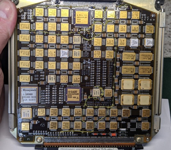
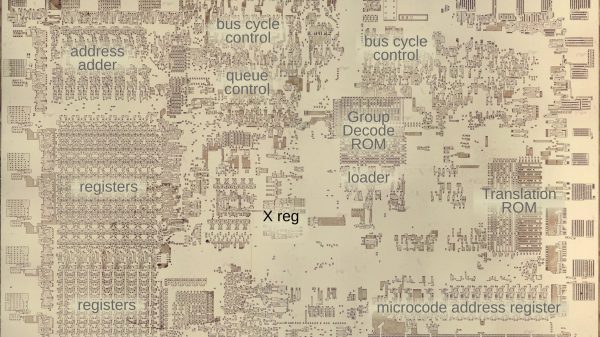
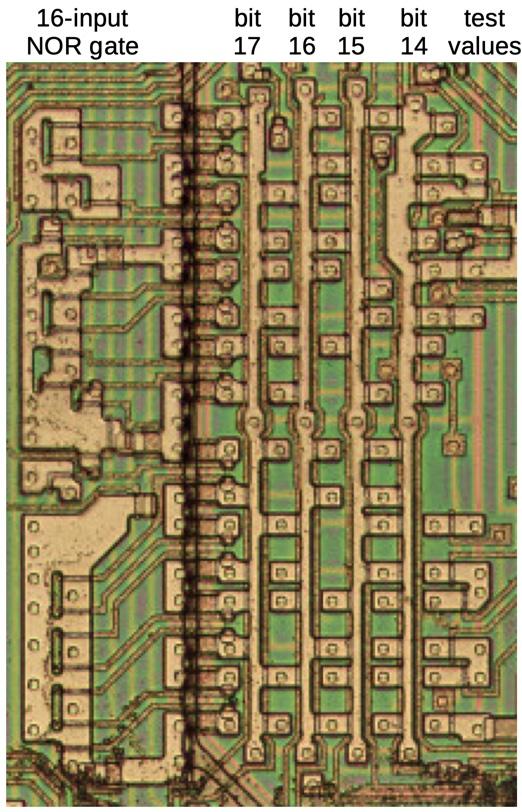
In the 1970s CPUs still had wildly different approaches to basic features, with the Intel 8086 being one of them. Whereas the 6502 used separate circuits for operations, and the Intel 8085 a clump of reconfigurable gates, the 8086 uses microcode that configures the ALU along with two lookup tables. This complexity is one of the reasons why the Intel 8086 is so unique, with [Ken Shirriff] taking an in-depth look at its workings on a functional and die-level.
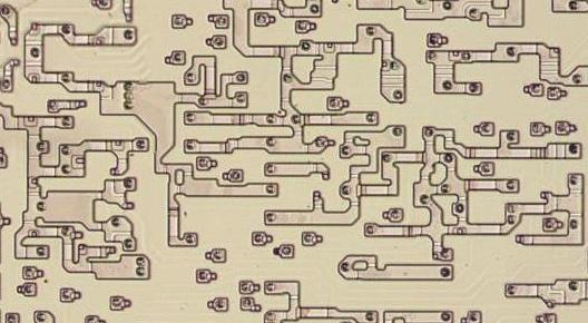
These lookup tables are used for the ALU configuration – as in the above schematic – making for a very flexible but also complex system, where the same microcode can be used by multiple instructions. This is effectively the very definition of a CISC-style processor, a legacy that the x86 ISA would carry with it even if the x86 CPUs today are internally more RISC-like. Decoding a single instruction and having it cascade into any of a variety of microcodes and control signals is very powerful, but comes with many trade-offs.
Of course, as semiconductor technology improved, along with design technologies, many of these trade-offs and disadvantages became less relevant. [Ken] also raises the interesting point that much of this ALU control technology is similar to that used in modern-day FPGAs, with their own reconfigurable logic using LUTs that allow for on-the-fly reconfiguration.