The Intel 8088 And 8086 Processor’s Instruction Prefetch Circuitry

The 8088 die under a microscope, with main functional blocks labeled. This photo shows the chip's single metal layer; the polysilicon and silicon are underneath. (Credit: Ken Shirriff)
The 8088 die under a microscope, with main functional blocks labeled. This photo shows the chip’s single metal layer; the polysilicon and silicon are underneath. (Credit: Ken Shirriff)

Cache prefetching is what allows processors to have data and/or instructions ready for use in a fast local cache rather than having to wait for a fetch request to trickle through to system RAM and back again. The Intel 8088  (and its big brother 8086) processor was among the first microprocessors to implement (instruction) prefetching in hardware, which [Ken Shirriff] has analyzed based on die images of this famous processor. This follows last year’s deep-dive into the 8086’s prefetching hardware, with (unsurprisingly) many similarities between these two microprocessors, as well as a few differences that are mostly due to the 8088’s cut-down 8-bit data bus.

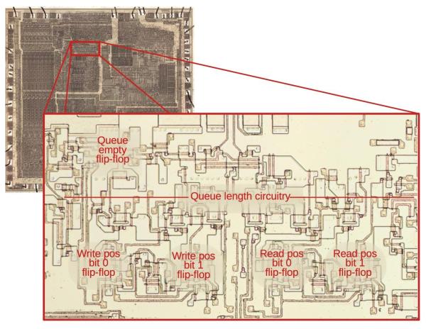
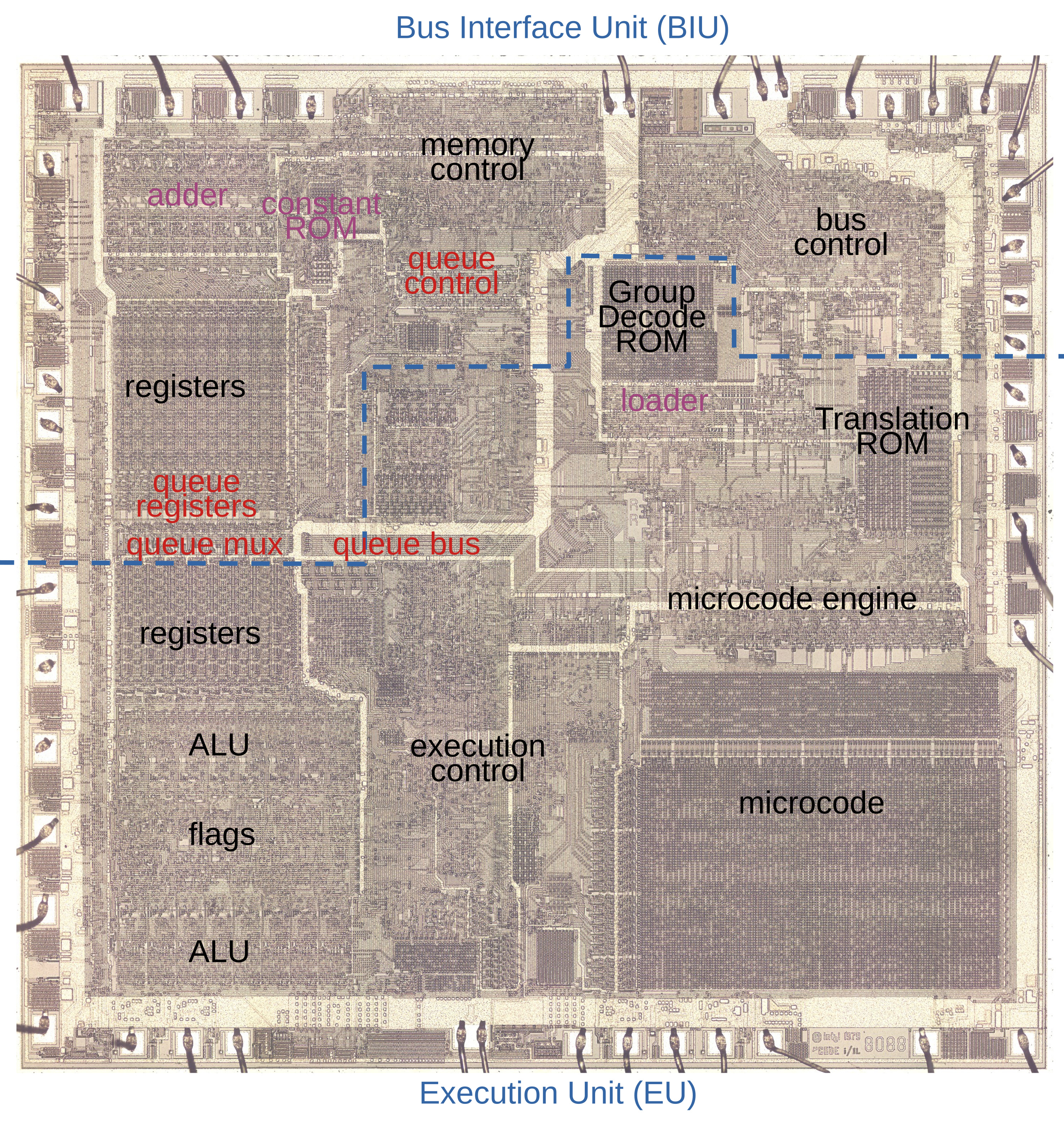
While the 8086 has 3 16-bit slots in the instruction prefetcher the 8088 gets 4 slots, each 8-bit. The prefetching hardware is part of the Bus Interface Unit (BIU), which effectively decouples the actual processor (Execution Unit, or EU) from the system RAM. While previous MPUs would be fully deterministic, with instructions being loaded from RAM and subsequently executed, the 8086 and 8088’s prefetching meant that such assumptions no longer were true. The added features in the BIU also meant that the instruction pointer (IP) and related registers moved to the BIU, while the ringbuffer logic around the queue had to somehow keep the queueing and pointer offsets into RAM working correctly.

Even though these days CPUs have much more complicated, multi-level caches that are measured in kilobytes and megabytes, it’s fascinating to see where it all began, with just a few bytes and relatively straight-forward hardware logic that you easily follow under a microscope.

NEC V20 - Konstantin Lanzet, CC BY-SA 3.0 via Wikimedia Commons

Intel V. NEC : The Case Of The V20’s Microcode

Back in the last century, Intel saw itself faced with a need to have ‘second source’ suppliers of its 8088 and 8086 processors, which saw NEC being roped in to be one of those alternative suppliers to keep Intel’s customers happy with the μPD 8086 and μPD 8088 offerings. Yet rather than using the Intel provided design files, NEC reverse-engineered the Intel CPUs, which led to Intel suing NEC over copying the microcode that forms an integral part of the x86 architecture. In a recent The Chip Letter entry by [Babbage] this case is covered in detail.

Although this lawsuit was cleared up, and NEC licensed the microcode from Intel, this didn’t stop NEC from creating their 8086 and 8088 compatible CPUs in the form of the V30 and V20 respectively. Although these were pin- and ISA-compatible, the internal microcode was distinct from the Intel microcode due to the different internal microarchitecture. In addition the V20 and V30 also had a special 8080 mode, that provided partial compatibility with Z80 software.

Long story short, Intel sued NEC with accusations of copyright infringement of the microcode, which led to years of legal battle, which both set many precedents about what is copyrightable about microcode, and ultimately cleared NEC to keep selling the V20 and V30. Unfortunately by then the 1990s had already arrived, and sales of the NEC chips had not been brisk due to the legal issues while Intel’s new 80386 CPU had taken the market by storm. This left NEC’s x86-compatible CPUs legacy mostly in the form of legal precedents, instead of the technological achievements it had hoped for, and set the tone for the computer market of the 1990s.

Thanks to [Stephen Walters] for the tip.

Finally, An Open-Source 8088 BIOS

The Intel 8088 is an interesting chip, being a variant of the more well-known 8086. Given the latter went on to lend its designation to one of the world’s favorite architectures, you can tell which of the two was higher status. Regardless, it was the 8088 that lived in the first IBM PC, and now, it even has its own open-source BIOS.

As with any BIOS, or Basic Input Output System, it’s charged with handling core low-level features for computers like the Micro 8088, Xi 8088, and NuXT. It handles chipset identification, keyboard and mouse communication, real-time clock, and display initialization, among other things.

Of course, BIOSes for 8088-based machines already exist. However, in many cases, they are considered to be proprietary code that cannot be freely shared over the internet. For retrocomputing enthusiasts, it’s of great value to have a open-source BIOS that can be shared, modified, and tweaked as needed to suit a wide variety of end uses.

If you want to learn more about the 8088 CPU, we’ve looked in depth at that topic before. Feel free to drop us a line with your own retro Intel hacks if you’ve got them kicking around!