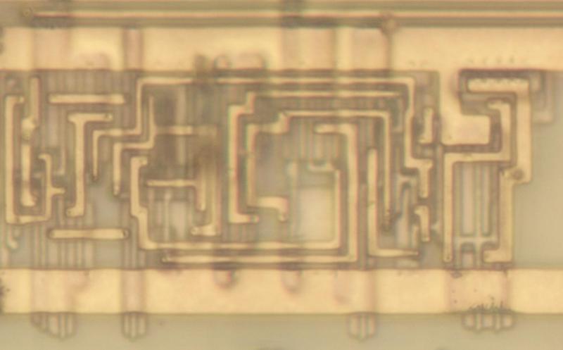
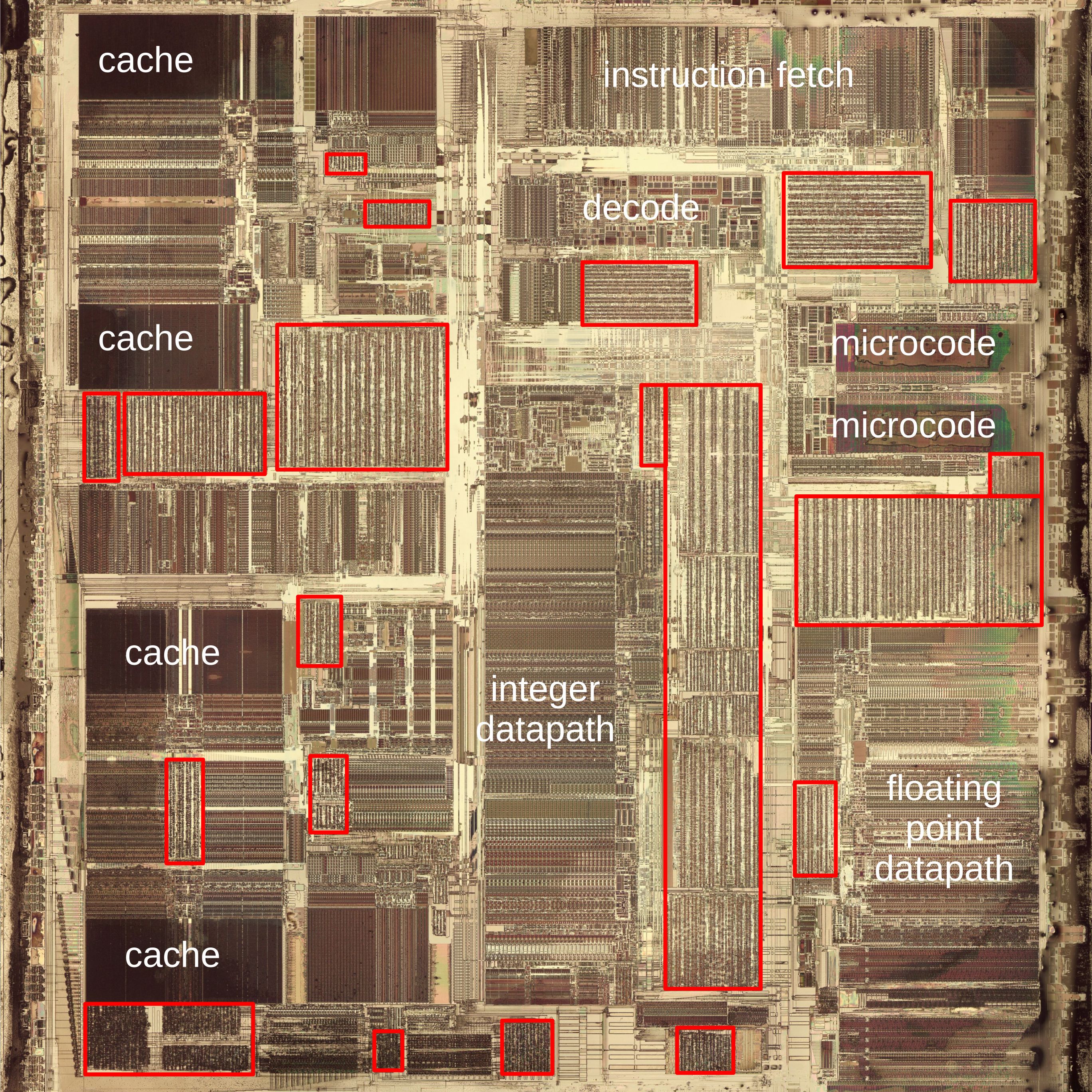
Whereas the CPUs and similar ASICs of the 1970s had their transistors laid out manually, with the move from LSI to VLSI, it became necessary to optimize the process of laying out the transistors and the metal interconnects between them. This resulted in the development of standard-cells: effectively batches of transistors with each a specific function that could be chained together. First simple and then more advanced auto-routing algorithms handled the placement and routing of these standard elements, leading to dies with easily recognizable structures under an optical microscope. Case in point an original (P54C) Intel Pentium, which [Ken Shirriff] took an in-depth look at.
Using a by now almost unimaginably large 600 nm process, the individual elements of these standard cells including their PMOS and NMOS components within the BiCMOS process can be readily identified and their structure reverse-engineered. What’s interesting about BiCMOS compared to CMOS is that the former allows for the use of bipolar junction transistors, which offer a range of speed, gain and output impedance advantages that are beneficial for some part of a CPU compared to CMOS. Over time BiCMOS’ advantages became less pronounced and was eventually abandoned.
All in all, this glimpse at the internals of a Pentium processor provides a fascinating snapshot of high-end Intel semiconductor prowess in the early 1990s.
(Top image: A D flip-flop in the Pentium. Credit: [Ken Shirriff] )


Amazing work! I love [ken sherriff]’s articles: loads of detailed photos you can zoom in and study if you want and good write-ups you can read and re-read bits at your leisure. So much better for technical documentation than a yt video.
Standard cells were always less efficient than a hand layout. Slower and required more space. But for some applications, say an instruction decoder, they were preferred. Basically a PLA. For things that were tricky and needed to be fast, an ALU for example, hand layout was still the way to go.
The full story is more complicated. For instance, a 32 x 32 multiplier requires a LOT of adders. The designer might hand lay out some adders optimized for delay-to-carry or delay-to-sum, and also both 3:2 and 5:3 adders, then design a schematic for the multiplier, then let the place-and-route software finish that portion of the job. Some software is also capable of taking the adders and a definition of a multiplier and creating a multiplier from the adders. At each automated stage, it’s possible to optimize for lowest delay of longest path. It’s a tedious and slow process, but hand-optimizing each adder would be overwhelming.
it seems to me like the difference between hand layout and using cells becomes kind of blurred. effectively, the ‘hand-layout adder’ is just another cell that they can use in the ALU. i mean, every cell starts out as hand layout to design the template the first time around. i’m just assuming no one wants to hand layout each adder like to conform around the geometric shape of nearby circuits! an adder is an adder is an adder, i hope.
The cited article states “But more importantly, long paths have higher resistance, slowing down the signals.” This is true, but in most cases it is not the dominant affect.
An output driving an input through a wire is to a first approximation an RC circuit. The resistance is the sum of the effective resistance of the driving FET plus the resistance of the wire; the resistance of the FET is usually much higher. The capacitance is the capacitance of the wire plus the capacitance of all gates driven. In most cases where wire length is a problem, it’s the added capacitance that’s the problem. This can be demonstrated when a problem shows up and it’s fixed by making the driving FETs stronger.
Good point, Chris. I’ve updated the article.
Please define your acronyms up front of you ever hope to reach a broader audience. First sentence had 4, most probably are ok with CPU but after that I stopped reading. Yeah yeah my problem but it’s literally jr high stuff about a topic sentence. Sorry-thanks
Sorry, gotta defend [Maya] here.
If you need Application Specific Integrated Circuit and (Very) Large Scale Integration spelled out to you, this simply isn’t an article you’re going to be interested in anyway.
This sentence is doing its job. If you don’t get it, move on, maybe come back when you do. It’s just not your time yet. I don’t think this article would benefit much from being rewritten to be more educational to a newcomer either. Like, that’d be jumping the shark.
HaD isn’t a “broader audience”. It’s a self-selecting niche and that’s OK.
Language barrier might be also a reason, maybe.
Not seldomly I’ve found myself in a situation were I knew a bit about the technical side, but was not fluent in the AE or BE slang.
I had no idea what ASAP, PITA or BS meant, for example.
Native speakers simply assume that everyone knows,
but we international people never had been told in English class in school.
Some technical terms are different in my mother language, too.
For example, the RCD (Residual-Current Device) is called FI (Fehlerstrom-Schutzschalter) in my language.
In computing, an extreme would have been “ZRE” (Zentrale Recheneinheit) or “ZVE” (Zentrale Verarbeitungseinheit) instead of “CPU” (Central Processing Unit).
Of course, both acronyms are being merely academic in nature these days.
In the 80s, they still had been used, though.
Same goes for “EDV” (Elektronische Datenverarbeitung).
It means electronic data processing and refers to computer use at the workplace.
It had been replaced by the term “IT” since internet became commonplace, but older folks don’t know what “IT” is.
Two convenient options:
1. If you are fine with adding tools to your browser:
https://addons.mozilla.org/de/firefox/addon/search-with-wikipedia/
2. If you prefer a little bit of work:
https://en.wikipedia.org/wiki/Wikipedia:Tools/Browser_tools/Mozilla_Firefox/URL_shortcut
(Yes, there are no other browsers.)
“Using a by now almost unimaginably large 600 nm process [..]”
Back in late 20th century it was still normal to measure in micrometers (µm) aka mircrons.
1000 nm = 1 µm
To give an idea, the 80386 microprocessor was made in 1,5 µm process.
The reason why modern proccesors are so tightly made is also because of built-in cache and complicated pipelining structures. They take up space.
And to be most efficient, they have to be close to the heart of the proccesor.
If that wasn’t the case, bigger structures could still be used well, I think.
Another reason is the voltage and operating frequency ratio.
Smaller structures allow for lower power consumption at an higher frequency (simultaneously).
Not that this says much in practice, though.
An old Z80 (NMOS) computer at 4 MHz required still less power a modern smartphone or Raspberry Pi does.
Same goes for an IBM PC from the 80s vs a modern PC.
Back then, the PSU was an 63W model – now a 350W, 500W or 750W PSU is being norm.
Progress isn’t always an one way road. ;)