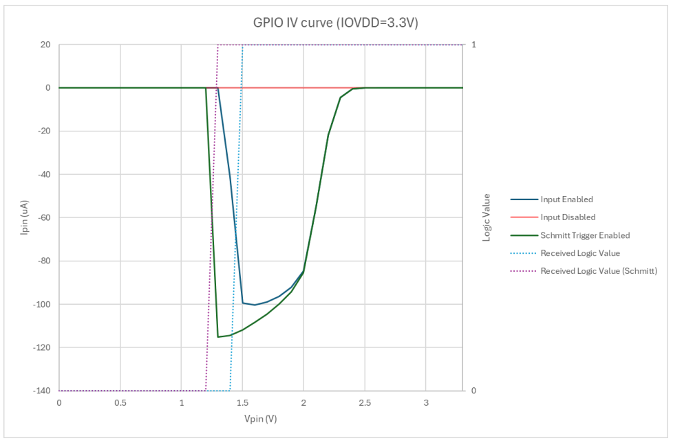
Although initially defined as an issue with GPIO inputs when configured with the internal pull-downs enabled, erratum RP2350-E9 has recently been redefined in the datasheet (page 1341) as a case of increased leakage current. As it is now understood since we previously reported, the issue occurs when a GPIO (0 – 47) is configured as input, the input buffer is enabled, and the pad voltage is somewhere between logic LOW and HIGH. In that case leakage current can be as high as 120 µA with IOVDD = 3.3 V. This leakage current is too much for the internal pull-up to overcome, ergo the need for an external pull-down: 8.2 kΩ or less, per the erratum. Disabling the input buffer will stop the leakage current, but reading the input requires re-enabling the buffer.
The upshot of this issue is that for input applications, the internal pull-downs are useless, and since PIO applications cannot toggle pad controls, the input buffer toggling workaround is not an option. ADC usage requires one to clear the GPIO input enable. In general any circuit that relies on floating pins or an internal pull-down resistor will be affected.
Although this should mean that the affected A2 stepping of the RP2350 MCU can still be used for applications where this is not an issue, and external pull-downs can be used as a ‘fix’ at the cost of extra power usage, it makes what should have been a drop-in replacement a troubled chip at best. At this point there have still been no definite statements from Raspberry Pi regarding a new (B0) stepping, leaving RP MCU users with the choice between the less flashy RP2040 and the buggy RP2350 for the foreseeable future.
Header: Thomas Amberg, CC BY-SA 2.0.


Still not gonna buy it.
That’s ok. I bought a few extra so you don’t have too :D :p .
From my point of few the programming tools are the same (2040 or 2350) whether Python or C/C++ . They are sure pushing the VS Code editor as an IDE though…. Luckily one can still use your own editor and use the cmd line to compile — so far.
https://www.galexander.org/rp2040
i programmed it ‘to the metal’ just to make sure i could, without using the sdk at all. i settled on a set up that doesn’t use anything from the sdk except a crc routine i cut-and-pasted. so i’m pretty optimistic that you’ll always be able to ditch the IDE. i’m pretty sure even if you want to use the sdk, the components are just .h / .o / .a libraries and you can use the standard tools with them.
they really did a pretty good job imo. i feel a lot more confident about being able to ditch the IDE / SDK than i do with arduino projects, at least.
As a long term Linux user it pains me to say I actually really like vs code. I feel gross to admitting it and need to go shower now.
customers also bought: TXB0108
(it fights you with up to +/-2 mA in between low and high levels)
That’s what it’s supposed to do? It’s an auto-direction sensing level shifter. You have to drive it hard to trigger it.
Those things can be both useful and a pain in the neck: too long a run, and a reflection will set the thing oscillating.
Undefined inputs are a common problem for low power designs. Many chips do the same thing with floating inputs where the voltage ends up in the hysteresis region of the input buffer. This HaD article seems to be confusing pull-up and -down though, so it’s unclear what the problem is.
Yeah, the errata says that it’s the pad pull-downs that are too weak to overcome the leakage, so the effective input voltage is about 2.2V. It says the pad pull-ups are stronger and work fine. That’s at 3.3 IOVDD. At 1.8 the leakage in effect becomes a pull-up.
thanks this is exactly the write up i was hoping to see from raspberry, and seems to confirm that shocking forum post.
the thing is, the specific strength of the rp2040 in my life (and i know i don’t speak for everyone!) is it’s the apex general purpose embeddable processor to rule them all and in the darkness bind them. it’s roughly as powerful as the stm32f1xx sort of things, roughly as well-documented, can be programmed to the metal or with an sdk, and it’s roughly as cheap as a PIC or imported stm32 clone, so i can buy a handful with no aim in mind.
there definitely are use cases where i wouldn’t mind if it draws a little current on the inputs. but there are other cases where i would care. i might resent the need to isolate it from its inputs (just a nuissance, maybe an extra transistor-resistor-resistor, maybe as much as 1mA per input). so i wouldn’t want a pile of them sitting around, not knowing which way the wind will blow me on the next project.
of course that’s no problem for me. the rp2040 is by far the most satisfactory chip i’ve had in that role yet :)
the rp2350 using a pare of spare risc cores makes me wonder if it would have been more sensible to have the backup cores dedicated to the rp2040 architecture. Of course, that wouldn’t have avoided this bug, since they both share the same pins.
But suppose it were possible to have half the pins on the old rp2040 design, and half the pins on the new rp2350 design. That way they would have a usable mcu, since it had been tested previously, and had the fix for the rp2040 adc bug rolled in.
If they are not prepared to build prototypes then that could be a better approach. microsoft does it too, every os they made was backward compatible. they made a great success out of supporting their customers.
Having half the pins on one controller, and half on another, and both sets of pins having different electrical characteristics would be incredibly painful as a designer that intends on using the device.
I think the issue here was more around an overly rapid time to market, and shortened validation / release window. They ideally would have internally characterised the part before selling any (with actual manufactured parts, not just sim), and when they identified the fault in the IO pad design would have pushed for a re-spin. Perhaps there’s even something they could have done to fix it ‘in-situ’ (i.e. laser ablation of pull down/bus hold) on the wafer.
The RP2350 is really pretty much the same architecture as the RP2040, but with better ARM cores, a couple of RISC cores, plus security and better power management. E9 is not an architecture issue, it’s a pad issue, and actually has been rather overblown by social media. Most people won’t have problems with it at all, the RP2350 very usable, as shown by the number of products using it already with no problems.
Ah, input leakage / shoot though, one of the historical annoyances of digital circuits.
A simple test anyone can do on a breadboard:
Program your favourite uC to define all I/O ports as inputs.
Connect them all together.
Add a potentiometer to it so you can vary the voltage on all pins between GND and Vcc.
Observe the power supply current (for example by adding a suitable shunt resistor in series with the power supply (Make sure you have your decoupling capacitors in place.
Very likely you will see a significant increase in power supply current when the voltages on the inuts is near half of the power supply voltage.
That is a different issue. The increased supply current is due to both the P and N MOS turning on at the same time. In the RP2350 the issue is current through the input pin.
I still don’t understand how this can happen. Is this leakage current through the protection diodes?
So is this going to be another bug where everyone refuses to tell shoppers which variant of the product they’re ordering?
When the Pi 4 USB-power bug was revealed, retailers douchily refused to tell you which board revision you’d be getting. They copped an attitude about it. I ended up doing the soldering to fix mine, but didn’t appreciate the attitude.
Given that there is no other variant, and isn’t likely to be in the foreseeable future… no. This isn’t a board level issue, it’s inside the chip itself.
But yeah, retailers deliberately misrepresenting their stock in order to flog it off is scumbag behaviour.
I hope they go back to the drawing board to fix this and add USB 2.0 while they are at it. The rp2040 worked shockingly well as a logic analyzer for a project of mine but it’s main limitation was front the data out.
With the added bandwidth, I think it could be a monster. I’m sure a bunch of other applications would benefit too.
One solution would be to compress or pre-process the data on the microcontroller.
Though the efficiency and latency of doing such could be more of a hassle than its worth.
USB 2 IP is a huge lump of silicon, and would make the price of the chip much higher, probably double. And why would you need to go back to the drawing board to fix a pad issue which has nothing to do with the architecture of the chip at all?
It’s a pity that it prevents use as a super-cheap logic analyser but I don’t think input buffers are such an awful thing to do. Having adjustable thresholds and some extra protection against abuse are significant improvements.
I believe the issue was everything was fine on the drawing board (that is, the design), but some component got replaced erroneously by a vendor in the implementation of the design. Still Raspberry Foundation’s fault for not catching it in (presumably) testing samples.
They should have aborted the rollout, issued a recall and/or sold off existing stock as faulty prototypes at a discount, issued an unequivocal apology saying they got it wrong and they’re doing everything they can to quickly fix it, and are right now restructuring their verification engineering. Instead, as expected, none of that happened. They continue with the launch at inflated prices, address the issue with useless documentation and social media, and when challenged their social army repeat the worn out excuse that “hardware is hard” and just throw in some resistors to fix the clearly broken silicon. Suffer kid.
At this stage with so many flops and failed launches it’s time for the Raspberry Pi leadership and their ripoff reseller board members to step down or face being escorted out the door.
And the worst part is that nobody asked for those new pads. They only had to change RP2040 to implement security domains. All they “needed to do” was to add secure boot.
RP2040 sorely lacks atomic instructions of two decade old Cortex M3/4 needing to use interrupt masking for critical sections resulting in more jitter.
For many many applications it also sorely lacks float instructions of M4. Also MPU is not present….
And no, 2 decades old M4 core is not much more pricier than M0+ that is why went ahead and licensed even much more powerful M33.
Don’t spread BS that nobody asked for better cores and it’s only about security features. Those features above I mentioned above are so absolutely huge that it’s marked as a different ARM architecture. thumb v6 vs v7
What an absurd statement. This is an easily worked around issue, no need for any massive recall or respin. Never mind the nonsense about overpricing, the chip is less than a dollar! Useless documentation? Nope. And what are these flops and failed launches? Pi seem to be making money so a call for leadership changes sounds like shilling for the competitors.
Yeah idk what he’s talking about with price/documentation, but I’m gonna have to STRONGLY disagree with you about how serious of an issue this is. This should 100% trigger a recall. Need 10 inputs with pull-downs? Suddenly your board has 10 more components that need to be designed around, ordered, and placed. There are lots of boards out there where, yes, adding 0402 resistors on every input pin would mean the board needs to be larger. That’s not to mention the power consumption – ~250 uA (once you account for the current through the external pull-down) PER INPUT could be huge for anything ultra low power, and would be a complete non-starter for a lot of my projects, where the inputs wouldn’t be able to source that much current without problems. Those problems alone are plenty enough to trigger a recall and respin for the chip. I was really looking forward to the rp2350, since the PIO blocks are really nice, and the cores are so much faster. Oh well.
It’s a relief to get this more in depth explanation, because it answers why the RP2350 was working just fine for my application (and probably why most other people who tested the RP2350 prior to launch didn’t catch this problem). All of the digital inputs into the RP2350 on my board have more than enough oompf to overcome the 120uA leakage current when driving low.
I think I am starting to understand what is happening, but is there a good example of what kind of circuit has an issue with this, and what does not, assuming you are not just putting a 8kohm resistor on every pin.
This “E9 bug” should not block you from buying and using the new RP2350. It should not be a real issue when you design your FW properly:
As I understand E9: it happens only if: a) you configure an input and let it “float” (open), and b) if you enable also the pull-down internally.
But “who as experienced FW designer” would do? Configuring an input with no driver on it (nothing from the outside), is not a “good design” (“never have inputs floating”).
As I understand E9: a) just if the pin is open AND the internal pull-down enabled – in this case, the “pin hangs” – not reliable what you read from it (and “hanging” in the “forbidden voltage zone”, driving a leakage current). It can “burn power”, if you use the external pull-down resistor recommended to overcome this “hang state” (just to real reliable a “0”).
b) but if your input is not open, there is an external driver providing a low impedance signal (as any external chip “sending” into input pin would do) – it will not show any effect. An external driver, even starting to drive a bit later, should “unlock” this state. The “E9 errata” does NOT say it would “hang forever” (just when input is kept floating).
Even with an external bi-directional level shifter (with auto-sensing, e.g. TXB 010x) it should work: just do not enable internal pull-down! During the phase where “nobody” is driving (when changing the pin to an input, before the external device starts driving, e.g. on a QSPI data line), why would you use an internal pull-down on this connection?
At the end, it becomes just an issue if you do this: a) configure an input but b) where nothing is connected to drive against it (“floating”), and c) you want to read “0” when open, therefore d) a pull-down internally. But who would do this? And it is not necessary: configure a pull-up and expect to read a “1” when open – and no issues.
Just avoid to use an “open input configured” (not driven from the outside) in combination with an internal “pull-down” enabled. No need to do anyway and all fine.
E9 is not a show stopper!
The leakage current is there whenever the input buffer is enabled, regardless of the state of the pull-down.
If you need a pull-down, the internal one is inadequate, so you must add an external stronger pull-down instead. If you want a high-impedance input, you have to add an external buffer.
Using it as a logic analyser is a good example, especially if the circuit that’s being analysed is some low power battery powered one.
They often have low signal currents in order to keep power consumption low.
Why would a low power circuit use high impedance drivers? Also if you were using it as a logic analyser why would you use pull up or pull down? These would likely change the behaviour of the signal you are trying to observe. LAs usually have high impedance inputs for this reason.
So I don’t this E9 errata will stop you using it in this way.
The E9 errata has been updated. The latching happens regardless of the pull-down being enabled.
On the github issue tracker, someone shows a trace of a sinewave becoming distorted by simply having the input enabled.
If the latched current is enough to effect what you are trying to observe, it will certainly be an issue.
But it was working in last version!