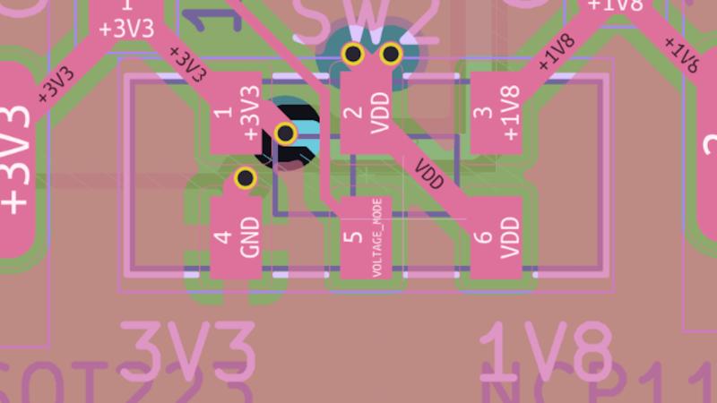
Ever want to build a RP2040 devboard that has everything you could ever want? Bad news, “everything” also means adding 1.8 V GPIO voltage support. The good news is that this write-up by [xenia] explains the process of adding a “3.3 V/1.8 V” slide switch onto your board.
Some parts are obvious, like the need to pick a flash chip that works at either voltage, for instance. Unfortunately, most of them don’t. But there’s more you’d be surprised by, like the crystal, a block where the recommended passives are tuned for 3.3 V, and you need to re-calculate them when it comes to 1.8 V operation – not great for swapping between voltages with a flick of a switch. Then, you need to adjust the bootloader to detect the voltage supplied — that’s where the fun begins, in large part. Modifying the second stage bootloader to support the flash chip being used proved to be quite a hassle, but we’re graced with a working implementation in the end.
All the details and insights laid out meticulously and to the point, well-deserved criticism of Raspberry Pi silicon and mask ROM design choices, code fully in Rust, and a success story in the end – [xenia]’s write-up has all you could wish for.
Want to learn more about the RP2040’s bootloader specifically? Then check this out — straight out of Cornell, a bootloader that’s also a self-spreading worm. Not only is it perfect for updating your entire RP2040 flock, but it also teaches you everything you could want to know about RP2040’s self-bringup process.


as so many things need to change for a steady working board, I would opt to bake two distinct versions with different color soldermask to differentiate them. blue for 3.3 and white for 1.8v
I was complaining (mostly to myself, but commenting here and there) about the lack of 1.8v VIO support in all boards.
Having read the article, I didn’t realize it was so complex. I thought the 2040 could be used for a cheap and simple JTAG/SWD cable due to PIO state machines and selectable IOVDD, but the slow USB and the complex IOVDD handling makes me look for a different platform. (FPGA and SWD interfaces sometimes drives out a VREF pin which you are expected to use for driving your IO pads so you can accommodate for 3.3v/2.5v/1.8v automatically).
Well, picoprobe can run SWD at 10Mhz without sweat with the USB it has. I was first using CH32V305 with high speed USB as cmsis-dap debugger with nrf52 and then found out picoprobe is good enough too (nrf52 swd is specced at 8MHz but works at 10 too).
For lower voltages you can use bidirectional level shifter, or nrf52840 can generate almost any voltage between 3.3 and 1.8 from 5V USB with its internal dc/dc regulator and use it for its gpio voltage, so if you know target voltage (like fpga with 2.5V) you can set it to that.
just to add about pricing, ch32v305 dongles (WCH Link E or the blue mini board clone) are $3-$5 on aliexpress and there is cmsis-dap with hs usb for it on github. cheapest nrf52840 now is probably the nice nano clone called super mini – ~$3 on aliexpress too, there is daplink branch for nrf52840 on github too.
That’s great!
I will have to disagree on the ‘everything’ part of ‘everything you could ever want’ though without 5V too.