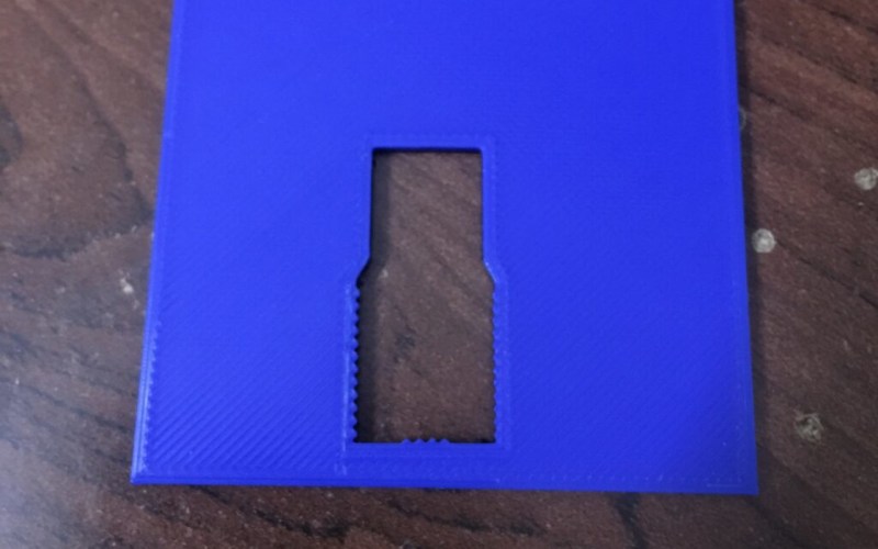
For many a hacker, stenciling a board for the first time is a game-changing experience – the solder joints you get, sure do give your PCB the aura of a mass-manufactured device. Now, you might not get a perfect print – and neither did [Atul R]. Not to worry, because if you have a 3D printer handy, he’s showing you how to design a 3D-printed frame using Blender and TinkerCAD, making your solder paste print well even if you’re trying to rest a giant stencil on top of a tiny board.
[Atul]’s situation was non-characteristic – the project is a 2mm thick PCB designed to plug right into a USB port, so the usual trick of using some scrap PCBs wouldn’t work, and using a 3D-printed frame turned out to be key. To get it done, he exported a .wrl from KiCad, processed it in Blender, and then designed a frame with help of TinkerCAD. These techniques, no doubt, will translate into your CAD of choice – especially if you go with .step export instead of .wrl.
This kind of frame design will get you far, especially for boards where the more common techniques fail – say, if you need to assemble a double-sided board and one side is already populated. Don’t have a stencil? You could surely make a 3D printed stencil, too, both for KiCad boards and for random Gerber files. Oh, and don’t forget this 3D-printable stencil alignment jig, while you’re at it – looks like it ought to save you quite a bit of trouble.


“Don’t have a stencil? You could surely make a 3D printed stencil, too…”
Thanks for that! It’s been quite a while since I last designed a PCB, and it was easy to solder by hand. But if I ever need to do the paste-and-stencil thing, I’ll definitely 3D print the stencil. Brilliant!
Why would you print a stencil when you order your PCB’s ? Stencils are free when you order from JLPCB
If you have read the linked article, you’d see that the 3d printed jig is a stencil+PCB holder, or stenciling frame in the electronic fabrication jargon, not a stencil on itself.
My stencil wasn’t free. What did you do to get a free stencil?
Are you sure? I just checked and stencils definitely are not free when using default settings so is there some combination of settings that gets them from free? The way it looks just now is $2 for 5 PCBs and $7.11 for the stencil.
Export board outline as DXF from KiCAD. Import into CAD. Add frame and extrude to 2mm thickness.
Or you could do it the hard way I suppose.
Or even simpler, let kikit do it. KiBot can trigger this as well. Point being, don’t do it manually when there’s tools that do it already :)
I Coincidentally just added support to my pipelIne component a few days ago!
https://gitlab.com/ci-includes/kici/-/blob/master/CHANGELOG.md?plain=1#L20
The neat thing about 3d printed stencils (atleast the kikit ones) is that they are self-aligning. E.g. they hold the pcb itself , so should alway align. Not sure how accurate the 3d pribter needs to be …
Sure, not everybody has one, I understand, but if you do have a laser cutter (I have a K40), you can laser cut the ‘paste layer’ in card stock (about 100um), and it lasts a few cycles (I got at least 5 cycles from mine) with reasonable results.
So i didnt properly rtfa, and he made a jig for the metal stencil. Kikit actually does both, a 3d printed stencil with a jig, and an metal alignment jig too.
I always 3d print a stencil jig for the PCB. Print a frame with a 1.6mm recess for the PCB and a 0.5mm recess for the stencil. I put holes instead of a big flat area so it uses heaps less filament and makes it easy to remove the PCB. Tape the stencil into the frame so it can hinge and production is ready 👍
I’ll often whip one up, especially for oddly shaped boards. If both sides need reflow, I’ll make it thicker and put a shoulder around the edges to suspend the board while I paste the second side. Done it for small 10x15mm up to 200x60mm.
I’ve got a write up on a PCB I designed that shows how well this works. Scroll down a bit and you call see the 3D printed jig holds the stencil perfectly in place for the PCB. It also allows for double sided placement.
https://hardingconcepts.com/bespoke-temperature/
If you are doing a lot of boards I recommend looking into having a “stencil8” jig made.
https://github.com/Hoektronics/Stencil8
It is just a grid of 2.5mm holes that are 10mm spaced in xy. Then you add at least 2 holes to your PCB (or PCB frame) and include them in the paste layers. Your stencils will come with the orientation holes and all you need to do is put the pcb on the jig and slide the stencil down on top.
In my case I use the framed stainless stencils with this method but I have in the past used the cheaper plastic and non framed stencils for this too.
I have even removed the stencil and put it back on and reapplied paste to an area I missed with success.
Currently, I am doing all my in house boards with this method including the V2 Smoothieboard which has a STM32H745 with a BGA package. Mostly 0402 parts.
Disclaimer: I have/do sell these plates. I am not the original designer. I recommend finding someone local to you to make one though. It is a good way to meet machinists. The majority of the cost is machine time since there are a ton of holes that need to be milled (milling preferred to drilling due to tolerances)…but it is not a difficult job at all.
oh that looks lovely! thank you for recommending it