If you compare a modern PCB with a typical 1980s PCB, you might notice — like [lcamtuf] did — that newer boards tend to have large areas of copper known as pours instead of empty space between traces. If you’ve ever wondered why this is, [lcamtuf] explains.
The answer isn’t as simple as you might think. In some cases, it is just because the designer is either copying the style of a different board or the design software makes it easy to do. However, the reason it caught on in the first place is a combination of high-speed circuitry and FCC RF emissions standards. But why do pours help with unintentional emissions and high-speed signals?
The answer lies in the inductance the pours add to the boards. Of course, there’s no free lunch. Adding inductance in this way also increases capacitance, which can be a bad thing.
The truth is, most of the boards we deal with would be fine with or without the pours. That’s a good thing, too, because the post illustrates how some common things can significantly reduce the effectiveness of the copper pours.
When we don’t send our boards out, we are usually more interested in removing copper. You also have to be careful when you want your PCB to radiate.


I mostly use pours to conserve the etching solution.
That was my first thought, the less copper you remove the longer it will last.
And that applies to large board houses where the etchant is a “hazardous waste” that has to be disposed of.
A look at the composition of most etching solutions does not make me feel like the term “hazardous waste” is invalid for them. Not as awful as semiconductor etchants, but I hardly want to take a nice big spoonful of the stuff every morning with breakfast.
This is the original reason. Cost. Pours also help improve yields since the prolonged etching necessary to remove large pours, leads to undercut on your traces, and eventually it’ll eat through.
yup, cost. Follow the path of the money as usual.
Not to mention in the past you might have to manually draw that pour with ink by hand!
Fine if you have a final circuit. Less so if you might want to use that space for a component in a future revision.
Most PCB fabs prefer as much copper pours as possible so their stuff lasts longer. I always added pours, tied to ground, because it costs nothing more than a few seconds
You may save on etching solution but you lose more in plating. It kind of balances out.
The board is already plated. The cost of the pour is already baked into the raw materials. The only way to “recover” this copper would be to recover it out of the etching solution and reconstitute it as pure copper. Then send it back to the substrate manufacturer as raw input material.
You really don’t understand PCB construction do you? Plating is how you get your vias to connect.
doing home etches, it also greatly reduces etch time. same holds true in an industrial setting. faster etch means you can produce a higher product volume in less time.
Well, with modern production methods it is more or less free RF shielding, so if it does no harm, why not.
It also reduces the interaction between circuits that share a common ground return path be reducing their shared resistance and inductance. At low frequencies the common ground return resistance dominates while at higher frequencies it’s the shared ground inductance that can cause problems.
Generally by using pours to generate the circuit grounds you can significantly reduce jitter and noise in both analog and digital systems.
i used to design network adapter cards in the 1990’s and the time you do not flood analog type component was under impedance transformers . If you look at any network card or front end to today with ethernet there is no copper pour under the signal transformers. The reason behind this was the copper flood used to bridge the transformer capacitivly so negating some of its purpose. Also seen in RF mixer circuits, do not flood under the ferrite ring.
Another factor is that with the move from wave-soldering of TH parts to reflow of SMDs, there is less risk of the thermal shock warping the board. Less copper to etch off also reduces cost in high-violume manufacture. And of course back in the days before CAD, pours were just hard to create with taped layouts.
On internal layers, pours are essential because it prevents differential expansion making the board twist. Even like 2 reflow cycles is bad enough to make a significant bend. Biggest mistake in my first 8 layer board. Always balance your copper, folks.
Beat me to it with “copper balance”
sample pics for others reading this: https://www.multi-circuit-boards.eu/en/pcb-design-aid/copper-balance.html
board sizes > 20 cm and thicker copper layers drastically magnify the imbalance problem. I’ve had a hastily designed 4L power PCB that showed curvature in both directions and made suspicious crackling noises when lightly flexing.
I’m under the impression that even local reworking made it bend even more out of shape.
It doesn’t even take thermal shock; the entire board bends with small changes in temperature, if there’s far more copper on one side than the other. They’ll arrive cup-shaped, straight out of the packaging.
Read it again.
Adding copper pours reduces inductance in power connections.
Adding copper pours increases the capacitance of power connections.
Unmentioned in the article is that copper pours help provide a defined impedance when designing transmission lines for high speed signals on PCBs.
This ^^
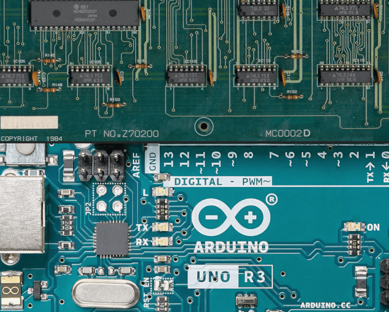
nice Amstrad CPC board on top!
I have also wondered if ’80s boards tended to have thicker copper, which would help power traces, but so far have been unable to confirm this.
In my experience they were roughly what we’d call one ounce copper, similar to current cheap boards.
I used to design PCBs’s from the late 1980’s for mixing sound consoles and we used 1oz copper or 35uM for most general pcb’s and 2 oz for Power supply PCBs to improve the current capacity. If you hold the the bare pcb laminate in your hand you notice the weight difference. Sometimes you see 2 oz in large old back plane PCB’s as well (like old telco and network equipment). Also longer etch times with 2oz copper so edge under cut of traces is worse.
I remember leaving as much copper as possible for better analog/digital ground planes
“Increased capacitance” is a good thing. Lower inductance and increased capacitance is exactly what you need to decouple power supplies.
Modern jellybean components are very fast, e.g. 74lvg1g* driving 2.5V into 50ohms with <300ps risetime. That requires excellent PSU decoupling, and Vcc+Gnd pours are very useful at removing the UHF/microwave frequencies where capacitors are inductive (i.e. Z rises with frequency).
You might, however, have to take into account the “cavity” resonance of solid Vcc+Gnd pours.
TL;DR is that power distribution networks (i.e. Vcc, Gnd) is a non-trivial topice with modern components.
Capacitance in power planes is only a good thing if it’s near switching loads otherwise it contributes to ringing signals. Power planes also cause excess capacitance in high speed signal traces which kills rise times and causes more ringing.
Please explain that ringing and the mechanism in more detail.
High speed signal traces have to be designed around transmission line concepts, which involve both capacitance and inductance.
Please give an example where it was not a transmission line but capacitance significantly slowed risetime; logic family, current source/sink capability, line length and impedance.
I2C bus, for example. Even the number of devices and length are limited by overall capacitance(including bus capacitance) if you follow the standard. 0.127mm wide trace over 0.127mm prepreg(and full plane) have ~1pF/cm capacitance which equals to 0.1 device/cm load approximately
Power/ground planes make it easier to make signal lines with a known constant impedance. How the signal line is terminated is part of what determines the nature of ringing. Generally, having a signal line unterminated (high impedance) leads to ringing. Terminating with a lumped capacitance (low dynamic impedance) leads to a different sort of ringing, which might be seen as degraded rise time.
I think the right answer here is “it depends”. Ground pour between high speed traces can be bad thing if they are not properly stitched. It’s better to use distance instead and no ground pour if the ground pour between high speed signals can not be properly via-stitched to ground. As previously mentioned, it can be beneficial as RF shielding, low inductance decoupling, and for balancing PCBs, just not as a blanket statement “always good”. I think both Zach Peterson and Rick Hartley have mentioned this in various videos online.
A signal’s return current does not take the path of least distance or resistance, but rather the path of least impedance which, because of mutual inductance, will be in the ground plane immediately below the trace, taking on the shape of the trace. It cannot do this when it hits the end of a poured area and suddenly has to find a detour to get around that gap. “Copper pours” (or fills) absolutely do not qualify as a ground plane. Not at all. A signal’s ground return current must run very close to the signal line, without interruptions. Copper pours will have interruptions, causing signal integrity problems. There is a way to use pours to supplement real planes; but if they’re not done correctly, they can actually make things worse, according to experts in the field like Rick Hartley, Eric Bogatin, and Suzie Web whose lectures you can see on Altium’s YouTube channel. Here’s another good video explanation from Eric Bogatin on Robert Feranec’s channel: “What Every PCB Designer Should Know – Return Current Path” 10/1/20: https://www.youtube.com/watch?v=icRzEZF3eZo Watch at least the first several minutes of Eric Bogatin describing what happens in a transmission line, and then see especially the area of approximately 28-30 minutes in.
They absolutely qualify as a ground plane if you make sure the return current’s got a continuous path. There’ll be impedance discontinuities if you have to change layers, obviously, but that’s not any different than a normal ground plane in a multilayer board, which also has discontinuities due to vias. Some of those discontinuities can be bigger than a layer change!
On a 2 layer board it can help to print out both layers and literally trace return current for signals. Sometimes it’s easy to see how to fix it. Yes, obviously, if you’ve got gaps and layer jumps it’s not going to be great at RF, but if you want a good clean RF path you keep everything the heck away from it anyway.
The one point you’re missing is that a copper pour doesn’t have to be ground, and power planes do not need to be as continuous. On a 4 layer board there are definitely cases where you’re better off making both interior layers ground and flooding top/bottom with power, stitching as needed. The decoupling caps will likely cover you well into the several-hundred MHz range, and the routes will have better-defined impedance without coupling through the power plane.
You apparently did not watch the videos. The return current doesn’t just need a continuous path; it needs to be a path that’s directly below the trace (unless you’re actually trying to make an antenna). If a trace goes off the edge of a poured area, even if only for a fraction of a mm before it gets back over another poured area, you’ll have a discontinuity, and degradation of signal integrity. As for the several hundred MHz, you’ll get that with fast logic, even at low clock speeds, because what we’re concerned with is the edge rates, ie, rise and fall times, not the clock rate. Jack Ganssle’s YouTube video, “I Only Probed the Board With a Scope – Why Did My Board Crash?” at https://www.youtube.com/watch?v=MJpDFnRQw8s, the part from about 2:20 to 3:00, graphically shows on a high-end oscilloscope that the ugly ringing remains unaffected as he turns the clock frequency up and down. I can recommend many more great videos, or just refer you to Altium’s channel, and also recommend Dr. Howard Johnson’s book, “High Speed Digital Design, A Handbook of Black Magic,” ISBN 978-81-317-1412-6.
It doesn’t need to be below the trace. If it did, coplanar waveguide structures wouldn’t work. Hell, you can route the return current with a trace if you want! That’s what tightly coupled DC balanced diff pairs are!
The reason why discontinuities matter is because it prevents an actual path. This is why you use layer change vias for ground when an RF signal changes layers if the reference plane for the new layer isn’t the same.
Yes, I’ve read Black Magic, and the followup. It’s not about magic rules. It’s about understanding that the signal is in the field between the trace and it’s return. If that path is clear, it’s fine.
I am familiar with coplanar waveguides, and have used them myself; but surprisingly, even in differential pairs running over a ground plane, most of the return current for each of the two lines runs through the ground plane, not its mate. I am also familiar with the matter of keeping continuity in the characteristic impedance when an RF (or fast digital, because of the edge rates, not the MHz) line is taken from one layer to another. The context here however is about copper pours, where a signal line goes off the edge of one poured area, over a gap (no matter how small that gap is), and on over another poured area, and the return current is forced to find a long detour, completely disqualifying pours as a ground plane.
In addition to the cost savings, another major reason for why they’re common now and weren’t before is that they offer really good shielding for high speed traces on internal layers. Back in the olden days multilayer boards were less common, but the benefit for emc/emi on modern boards when you can use them to basically surround your sensitive traces in a Faraday cafe of copper pours is significant.
I wouldn’t mind grabbing a drink at the Faraday Cafe. Catchy name
As a veteran PCB designer of 18 years doing RF boards I can say copper pours have a wide range of effects. Anything from shielding, better grounding, capacitance for power power, heat dissipation, even out plating, consistent reflow, controlling board warp, etc… However there is a dark side to the force. They can cause cross talk, ground loops, cupping, unintentional feed back loops, standing waves, impedance discontinuities and many more nasty things.
Only experience and awareness of potential issues can help you master them. In other words you need to push the limits, screw up alot, and resolve the problem alot. Once you do you can feel your way and let the force guide you.