We have all seen Printed Circuit Board (PCB) antennas: those squiggly bits of traces on PCBs connected often to a Bluetooth, WiFi or other wireless communication chip. On modules like for the ESP8266 and ESP32 platforms the PCB antennas are often integrated onto the module’s PCB, yet even with such a ready-made module it’s possible to completely destroy the effectiveness of this antenna. These and other design issues are discussed in this article by [MisterHW].
It covers a range of examples of poor design, from having ground fill underneath an antenna, to having metal near the antenna, to putting dielectric materials near or on top of the antenna. The effect of all of these issues is generally to attenuate the signal, sometimes to the point where the antenna is essentially useless.
Ultimately, the best PCB antenna design is one where there is no nearby copper fill, and there are no traces running near or on layers below the antenna. After all, any metal trace or component is an antenna, and any dielectric materials will dampen the signal. Fortunately, there is e.g. a free KiCad library with ready-to-use PCB antenna designs to help one get started with a custom design, as well as many other resources, covered in the article.
If you want to get really professional about checking the effectiveness of an antenna design, you’ll want to use a Network Vector Analyzer. These will also help you with tuning the capacitors used with the PCB antenna.
(Featured image: PCB antenna rendered useless by overly enthusiastic copper fill.)


You forgot to mention that holding wrong is another no no.
You meant Vector Network Analyzer (VNA).
Okay so like a daughter board antenna with no other traces is most ideal from a performance only standpoint, that way the antenna has the least amount of obstacles to compete with. I believe that a antenna jack would be a better option then. The PCB antennas are suited for space saving and there is a trade off there unfortunately and it’s performance in this case. Does the unit require long distance Radio broadcasts or is it just receiving? There are many factors in antenna performance! You never fail, simply finding ways to not succeed.
The instant you use a different antenna, you need to redo FCC Qual. The inbuilt antennas can come with their own FCC IDs.
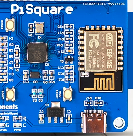
The example PCB must have been designed by someone who didn’t bother to read the datasheet. It’s very clear about the clear area required near the antenna, and there was plenty of space, if had just rotated the module 180 degrees and moved it up towards the edge of the PCB.
unfortunately it’s a commercial board. seems to cost £9
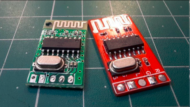
Not the first board I’ve seen to mount an ESP* in the middle of a ground plane
I have the “megacell charger” – Yeah the same. An ESP8266 smack dab in the middle of the PCB with a groundplane. And it’s not even first revision of PCB. It’s soo freaking stupid. And yes, the WiFi-range is c*ap.
But it worked for me in testing!! /s
This is one of those areas where modern tools and services allow anyone to create designs with minimal skill required. The creator obviously understand electronics, but can be forgiven for not being aware of antenna design requirements, as it’s a complicated area of design few really understand.
As it’s a Kickstarter, it looks the author simply never realised the design need, and didn’t get anyone who was aware of it to review. That’s the failure right there, and hopefully something they’ll do better at in future
Perhaps the sheer number of examples allows to draw the conclusion that handling designs with antennas is a conscious process. Antennas are not components that need to be “somewhere on a board”, although chip versions by their nature try to tell that story.
A first step in building an understanding for PCB antennas is to consider:
An inverted-F antenna is adjacent to a ground plane edge, and the edge is part of the antenna design.
The PCB it is manufactured on is part of the antenna design.
The empty space above and below it is part of the antenna design.
(I know it’s silly in retrospect when there is clear documentation on it, but documentation does not prevent mistakes, routine does)
Anyone with an even a very basic understanding of RF will know that placement will not perform well.
Exactly, the writer is clearly thinks they are aiming the best performance. The designers of the board don’t want that, of course. They just want a bit of wireless communication. This may be their very first RF board they have to o sell because they made also a mistake of making a good amount of them. You as a smart user can decide to buy it or not too
Actually, it’s potentially illegal to sell. The point of modules is they have been tested to ensure they meet radio emissions standards/laws. By not using them correctly they detune the antenna and potentially change the emissions so they are no longer compliant.
Actually, you can make a backfire antenna with a groundplane…
helpful, thanks.
Don’t put the antenna on the PCB. Problem solved.
Sometimes (wireless mouse) there’s nowhere else to put it.
Another tip — if you’re doing this for a product, the RF module vendor’s applications engineer may be able to take your PCB layout and run it through an RF analysis software package. Both time I did a PCB antenna, that’s what happened. We couldn’t justify owning the $$k tool ourselves, but they were happy to check out layout, offered etch change suggestions and recommended values for matching components.
Having ground plane near an antenna may impair it or it may be necessary for proper antenna function. Same goes for dielectric. Take a look at the little squiggly antennas on the typical ESP8256 module. Those are dimensioned the way they are because of the dielectric value of the PCB material. High end PCB material made for RF work is carefully characterized for dielectric constant so that traces and other elements can be properly sized. There are whole classes of antennas that rely on precisely controlled dielectric environments–including some which use the dielectric’s shape to help define the radiation pattern.
What you want to avoid is breaking the assumptions built into the antenna design. That’s where you run into problems. Like that poor little burried ESP-12 module imprisoned in the middle of a ground pour. Please, just rotate it 90 degrees and hang the antenna off the PCB!
Every SOC with RF TX capability should have a simple VSWR meter built in and send random insulting notes via UART if the ratio is worse than, say, 3.
Adding a VSWR meter would insert loss into the RF path.
As things stand, I wouldn’t be surprised if manufacturers gave up on the need for RF design knowledge and went straight to adding aperture tuning based on RSSI. Cuts out the middle-man.
https://www.microwavejournal.com/articles/21283-a-method-to-design-an-aperture-tuned-antenna-using-a-mems-digital-variable-capacitor
Any time I see examples with thermal reliefs on components on the RF path I have to cringe. Every thermal spoke is an inductor and it does effect the circuit. (I have 18 years experience doing RF layout)
This brings all new meaning to the old term:
Wireless Antenna.
:)
Fortunately you can now get ESP32 with an external antenna that plugs into a mini socket on the board.
There’s always a catch, and modules certified with an on-board antenna can save you a ton of money. It’s another case of “why we cannot have nice things”. I personally ran into this with u.blox bluetooth modules, but the same applies to Wifi modules. Want an external antenna? I’m not sure the regulations have been relaxed in the meantime – last time I checked that meant you’d have to re-qualify that exact combination of module and antenna.
https://linxtechnologies.com/wp/blog-post/antenna-fcc-certification/
Here’s what needed to be delivered in terms of experiments and documentation for the ESP12F module:
https://fcc.report/FCC-ID/2AHMR-ESP12F
And ESP8266 as well (ESP-07 and S models at least).
https://www.nicerf.com/articles/detail/antenna-length-frequency-and-wavelength.html#:~:text=The%20length%20of%20the%20antenna,the%20antenna%20can%20be%20made.
The rf carier signal charstaristics determin the length of the antenne. the antenne is just a resonator for that signal. the sin wave can be seen as a few millimeters. and after the radio frequency is choosen. then the length of the antenna can be made, wheiter bend or not. for optimal design, can be choosen for 1 or 2 antenna’s with the same length in total of the signal. sometimes it depends also from wich direction the signal come from. from the side or from upfront.