Once a printed circuit board (PCB) has been assembled it’s rather hard to look inside of it, which can be problematic when you have e.g. a multilayer PCB of an (old) system that you really would like to dissect to take a look at the copper layers and other details that may be hidden inside, such as Easter eggs on inner layers. [Lorentio Brodeso]’s ‘LACED’ project offers one such method, using both chemical etching and a 5 Watt diode engraving laser to remove the soldermask, copper and FR4 fiberglass layers.
This project uses sodium hydroxide (NaOH) to dissolve the solder mask, followed by hydrogen chloride (HCl) and hydrogen peroxide (H2O2) to dissolve the copper in each layer. The engraving laser is used for the removing of the FR4 material. Despite the ‘LACED’ acronym standing for Laser-Controlled Etching and Delayering, the chemical method(s) and laser steps are performed independently from each other.
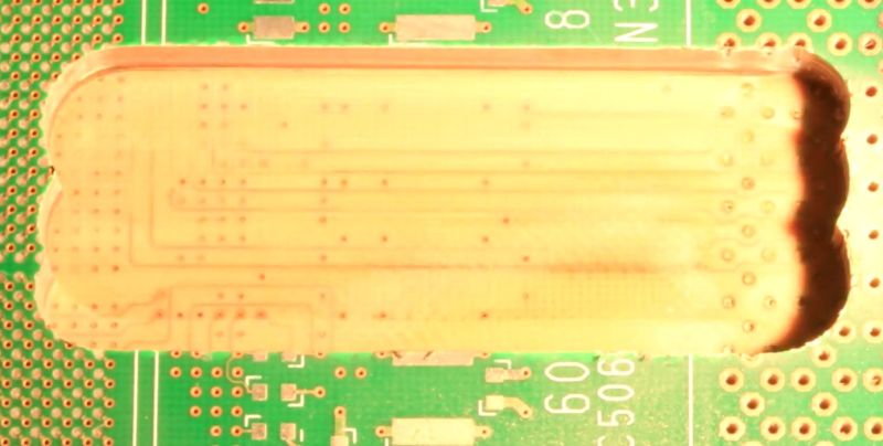
This makes it in a way a variation on the more traditional CNC-based method, as demonstrated by [mikeselectricstuff] (as shown in the top image) back in 2016, alongside the detailed setup video of how a multi-layer PCB was peeled back with enough resolution to make out each successive copper and fiberglass layer.
The term ‘laser-assisted etching’ is generally used for e.g. glass etching with HF or KOH in combination with a femtosecond laser to realize high-resolution optical features, ‘selective laser etching’ where the etchant is assisted by the laser-affected material, or the related laser-induced etching of hard & brittle materials. Beyond these there is a whole world of laser-induced or laser-activated etching or functionalized methods, all of which require that the chemical- and laser-based steps are used in unison.
Aside from this, the use of chemicals to etch away soldermask and copper does of course leave one with a similar messy clean-up as when etching new PCBs, but it can provide more control due to the selective etching, as a CNC’s carbide bit will just as happily chew through FR4 as copper. When reverse-engineering a PCB you will have to pick whatever method works best for you.
Top image: Exposed inner copper on multilayer PCB. (Credit: mikeselectricstuff, YouTube)


I’m Lorentio Brodesco, the creator of LACED, and I feel compelled to leave a response because, frankly, this article significantly underrepresents the essence and technical depth of the project.
Key elements are entirely omitted — most notably, the achieved vertical resolution of 3–10 microns per pass, which was a central breakthrough. The method is portrayed as “just another approach” and is inaccurately compared to mechanical CNC milling, despite the fact that LACED is opto-chemical, non-mechanical, and far more precise than any consumer-grade mill.
Furthermore, it is not mentioned that the entire setup used to achieve this level of precision costs under €200, making it one of the most accessible methods available today for PCB layer isolation and analysis. The article also does not consider that the frequently referenced carbide-tipped CNC bit is fundamentally unsuitable for this kind of analysis: it cuts FR4 and copper indiscriminately, which introduces a serious risk of mechanical damage to underlying traces. The laser approach, on the other hand, does not ablate copper, allowing controlled removal of dielectric layers without compromising signal paths.
Nearly half of the article veers off-topic into a discussion about mechanical engraving, completely missing the point of LACED’s methodology and the 30+ pages of open-source documentation that outline its scientific basis, reproducibility, and application to multi-layer PCBs.
This is not a minor tweak to an old technique. LACED is a novel, accessible process combining low-cost lasers with controlled chemical etching — offering micron-level layer separation, compatible with high-layer-count PCBs, and achievable by anyone willing to experiment carefully.
I respect the effort to showcase new work, but I’d encourage a deeper technical look when publishing. This project wasn’t meant to be a curiosity — it’s meant to be a tool. And it already is.
Thank you for writing this. I have similar thoughts about the majority of hackaday articles. They are very often interesting, but I wish the author had spent more time on truly understanding the subject – and then communicate it.
On the other hand, Hackaday articles don’t need to be a duplicate of the material on the project page itself. Explaining the significance from another perspective and comparing it to alternatives is worthwhile itself.
Man, KIs are getting so good. I wouldn’t be able to say “I am butthurt that I’m less significant than I think.”
The walls of text and the aggressive marketing (see below) of this project on multiple sites and probably forums and wasn’t enough apparently, since despite the undoubtedly lengthy interactions, the person behind it still hasn’t gotten the hint.
I’m not going to let ChatGPT render some refutation to the above, since I just don’t have the nerve for it, but as someone who’s looked into actual laser-assisted chemical ething (LACE (1)): the name “laced” alone feels deliberately misleading.
You had the oppportunity to present the board imaging and said: all you need is cupric chloride etchant (2), a sander and a vacuum cleaner, have at it”. Maybe cut off a section, polish the side and precisely measure the copper and prepreg thicknesses and you’re good to go, as is being done regularly. No lasers needed.
Also, when you use LLMs, you don’t get to brag about “30+ pages” about two established and quasi trivial processes that do not meet any criteria for novelty, neither individually nor used sequentially.
(1) https://hackaday.io/project/156522-step-and-scan-digital-microlithography/log/146551-laser-assisted-chemical-etching
(2) https://www.instructables.com/Stop-using-Ferric-Chloride-etchant!–A-better-etc/
—
– hackaday tips line
– https://bitbuilt.net/forums/index.php?threads/laced-%E2%80%93-%C2%B5precision-pcb-delayering-for-under-%E2%82%AC200.6908/
-https://www.reddit.com/r/retrogaming/comments/1kjrhon/from_sanding_a_ps1_motherboard_by_hand_to/
…
Thanks for your pointers. I expected quite a bit from the project after reading OP’s comment. While the project is interesting, it took me several passes to understand he is not using lasers to assist chemical etching. It’s ‘just’ etching the board to remove the copper, and revealing the next copper layer with a laser.
At ten passes, 15 minute per pass, the whole process takes over a day to complete, which isn’t a problem, but it’s not recognized in the text that the process is extremely tedious. Mostly as these aren’t the lasers you should leave running without supervision, nor without the proper enclosure, ventilation, and PPE.
Don’t worry. Nobody actually reads the articles. They’re mostly just grandstanding in the comments. Which nobody reads either.
Thanks for all the great work and chiming in on why this is more than just another reversing technique. After sanding a few pcbs to reverse them, I am very excited about this option, especially that it is relatively nontoxic and very affordable. I got the laser you used and set it up last night.
Lorentio neatly pre-empted much of what I was going to say: “Why would you want to use a complex, time consuming process with somewhat hazardous chemistry AND destroy the board in the process, when you could just x-ray it?” (the answers are: accessibility, cost, and resolution, in case it’s not obvious).
You’re still left with sludge in the place of a board at the end of the process, but this is something patient people without access to an x-ray system can do.