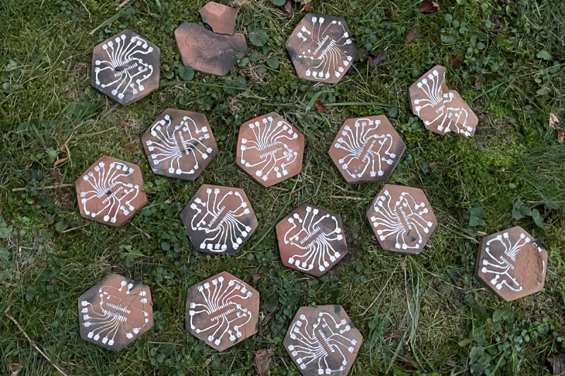
When we see an extremely DIY project, you always get someone who jokes “well, you didn’t collect sand and grow your own silicon”. [Patrícia J. Reis] and [Stefanie Wuschitz] did the next best thing: they collected local soil, sieved it down, and fired their own clay PCB substrates over a campfire. They even built up a portable lab-in-a-backpack so they could go from dirt to blinky in the woods with just what they carried on their back.
This project is half art, half extreme DIY practice, and half environmental consciousness. (There’s overlap.) And the clay PCB is just part of the equation. In an effort to approach zero-impact electronics, they pulled ATmega328s out of broken Arduino boards, and otherwise “urban mined” everything else they could: desoldering components from the junk bin along the way.
The traces themselves turned out to be the tricky bit. They are embossed with a 3D print into the clay and then filled with silver before firing. The pair experimented with a variety of the obvious metals, and silver was the only candidate that was both conductive and could be soldered to after firing. Where did they get the silver dust? They bought silver paint from a local supplier who makes it out of waste dust from a jewelry factory. We suppose they could have sat around the campfire with some old silver spoons and a file, but you have to draw the line somewhere. These are clay PCBs, people!
Is this practical? Nope! It’s an experiment to see how far they can take the idea of the pre-industrial, or maybe post-apocalyptic, Arduino. [Patrícia] mentions that the firing is particularly unreliable, and variations in thickness and firing temperature lead to many cracks. It’s an art that takes experience to master.
We actually got to see the working demos in the flesh, and can confirm that they did indeed blink! Plus, they look super cool. The video from their talk is heavy on theory, but we love the practice.
DIY clay PCBs make our own toner transfer techniques look like something out of the Jetsons.


This is just the aesthetic of environmentalism, not environmentalism itself. The chips are still made of epoxy and silicon and require billions of dollars worth of infrastructure! They need to think about this some more before bothering everyone else with their nonsense. These people are just making actual environmentalism look bad.
And I thought the Flintstones did the PCBs.
They did have a CRT TV so obviously they found a way to turn clay and scrap into working TV
Sadly that is 99% of the environmentalism in the current era.
Its a tech problem, both the origins and its solutions. It can’t go anywhere while humanities and social sciences focused leadership works on social issues other intangible before addressing the actual technical solutions.
Absolutely no hate to anyone. Everyone means the best, their methods may be different. Sadly while valuable, social solutions alone cannot prevail. Engineering can only be ignored for so long
Yeah, environmentalism in 2025 is basically an industrial consortium laundered through a lot of internationals and NGOs to promote the production of far more expensive and profitable hardware at the expense of massive pollution for the illusion of being sustainable. Sustainability, even though it’s theoretically possible, is precluded by the base motive of the consortium trying to increase its margins. It will never happen in its current state.
I know this from personal insider experience. These people will burn the world down , not merely to profit from it, but also to have the sanctimonious frisson of being superior to those other guys who also want to burn the world down to profit from it. Also the sadistic frisson of making millions of regular people (whom they venomously hate) tighten their belts.
And one of the saddest parts is the scientific plausibility of some of these ideas is abused as cynical cover to shut people up who point out they aren’t doing what they say they’re doing, that they’re the same as before, just another rival gang vying for the top position.
“Everyone means the best” is either a very naive or very dishonest thing to say. The Hollywood elites, shouting about sea levels rising while they buy multi-million dollar beach houses, telling us to drive smaller cars while they take private jets to get a latte, definitely don’t “mean the best” for anyone but themselves as they pander to nihilist, anti-human lunatics. The same goes double for the lawmakers and NGOs, burning jet fuel by the kiloton so they can discuss how to take away freedoms and gain more power and tax money to waste.
Not really, this is from an environmental POV massively better than the usual PCB substrates.
Yes its not a complete replacement of all the somewhat toxic and high complexity industries that usually go into circuit boards, but using salvaged chips is still another winner environmentally.
Obviously this is more art and proof of concept than serious, but still its hitting lots of good points, with reuse being better than recycle etc and avoiding fibreglass is not a bad thing environmentally.
But ceramic PCBs already exist! They’re just expensive. Still cheaper than all that silver they used, though. The problem isn’t that we don’t know how to make environmentally-friendly devices, it’s that optimization inevitably leads to hell. Cheap and nasty sells better than expensive and clean. It’s a tale as old as evolution. If you want to take on environmental pollution, you need to take on efficiency itself as a concept.
For more reading on this, see the Jevons paradox:
https://en.wikipedia.org/wiki/Jevons_paradox
Though the silver was also at least pseudo reused rather than strictly recycled so is actually somewhat kinder from an environmental point of view. The monatary value does not directly equate it is still effective enough, at least if the circuit actually did something useful it would be environmentally pretty close to optimal. It is taking waste and reusing it, taking local materials and simple processes for the rest, all disconnected from the profit is everything burn the world of your usual suppliers…
And a large part of taking on cheap and nasty sells better is getting folks to actually realise the story of their purchase, or even better become part of it so they are personally invested and now know they can create and really own it, modify etc.
Then with the goal of making it ecologically sound as well as just not cheap and nasty you need that story to include local reuse and recycling and materials – so rather than buy prefabbed double sided FR4 that was made in big industrial units in places that probably don’t have to worry much about cleaning up properly, and from raw materials as cheap as they can source (so likely just as damaging or worse).
But as we see in reality, people avoid this behavior at all costs (because it is inefficient). Efficiency causes consumption causes pollution. Yeast in a petri dish, or humans on earth; it’s the same story either way.
Do we really!? I’d say that is an untenable argument given we were talking about an example of folks actually getting involved and doing it, then sharing their story not just understanding the story. And the successes of things like Pine64, Framework, Fairphone, the FOSS world in general (etc etc, as there are so many examples) show there are plenty of folks out there that at least buy into the story of a better solution if they are not actively contributing to making it. Obviously can’t claim everyone on Earth is engaging, but avoid at all costs is evidentially false, the furthest you can go on that sort of idea IMO remotely defensibly is “people selectively avoid/engage in this behaviour in only parts of the their lives”.
Also is it really inefficient if you enjoy the process? Seems like a much more efficient option to me than consuming yet more low effort for maximum profit slop to fill your time…
” bothering people with their nonsense” who, pray, was bothered by this?
Me, personally, for accidentally reading and watching it. The audience, for having to sit politely through it, or (in the worst case) if the audience enjoyed it, their friends and family for having to hear about it later.
It’s an entire butterfly effect of academic navel-gazing. Who knows how much harm was caused, all things considered?
sigh… I’ll post on some of the technical details later, but Really? You are offended by someone doing an art/exploratory piece about making their own ceramic PCB’s? Ceramic PCBs and ceramic hybrid circuits, are nothing new. That said, rolling your own from dirt to finished product is nice ;-)I’m glad they did this, and if you are offended, why are you reading anything on Hackaday. Doing something OUT There is definitely the jab mere…
This isn’t a “butterfly effect” (whatever that means) of academic navel-gazing. It’s a high-horse from which you’re catastrophizing. This kind of thing has always been and will always be a part of our society. Academics like to make art. People like to make their own . That’s what this site is all about.
A lot of times people try to justify their esoteric pursuits with specious claims. So what?
It’s way better than, say, people who shoot guns as a hobby, then justify that hobby with specious BS, then become preppers who constantly compare limiting access to guns for people with domestic violence backgrounds to “tyrannical government taking away ALL our guns” or whatever…
I wasn’t bothered by the technical content but mixing woke philosophy, feminism, and environmentalism into the video was annoying.
Its the same thing as in electric cars: even if its still polluting, take into account that the PCB itself is still 20 or 40 kg of CO2 eq per square meter (depends on the study), plus the various wastes. For an example arduino uno (what they wanted to make), it would be 110g CO2eq. for the PCB.
On the other hand, A STM32 (idk for a 328P) is 120g of CO2. Maybe the transport is not negligible, but the PCB is as polluting (and probably more) than the chip itself.
Its not an aesthetic, any way of diminishing the environmental impact of PCBs can reduce the impact of IT (even if its whole impact isn’t really important in the world), even if its not done mainly for economic and reliability reasons.
Yes chips fabs are polluting and expensive, but they make a lot of chips.
And what were the CO2 emissions of their campfire? Probably higher than that!
Wood fire is carbon neutral (I’m assuming afterwards they wandered off and planted a tree).
Even if they didn’t plant anything new as long as they are not burning a forest down at industrial scales the forest will do the job for you – it is in theory a self repairing system that is forever generating more dead wood you can collect to burn entirely on its own. No lasting harm is done.
No it’s not. If you burn a forest, and look at a “multiple of your life” time, it’s probably neutral when all the tree and all the microbial ecosystem will have resumed.
But in the current scheme of things, you’re freeing more CO2 to the atmosphere than the tree around can capture. And the fact that everyone is doing this, right now, make the ecosystem instable and more and more unlikely to recover and re-absorb it.
In short, the CO2 from your burnt stick is not different from the CO2 of your burnt fuel of your car, so the tree that are, in your logic, supposed to absorb it back will just pick the CO2 from your car (because there’s more of it now), leaving the CO2 of your stick poisoning you.
It would have been ten times better if you hadn’t burn that stick, the CO2 wouldn’t exist at first, since it’s stored as cellulose and lignin in your stick and doesn’t help disturbing the life condition we know of.
It would be if it would not be cut down all around the world like there is no tomorrow. (There will not be with this pace…)
so they should have made it out of homebrew vacuum tubes?
That would be better, and a relay oscillator would be better still, but the best would be not to build it at all (seeing as the circuit does nothing useful).
As they said they used salvaged already existing chips that would be massively masively worse. Making your own tubes is going to be insanely energy intensive, and require loads of relatively high cost new or recycled resources compared to desoldering and reusing existing chips from e-waste…
I do agree on the lack of practical purpose in the end results making it better to not build it in the strictest sense. However before you can make inevitably more complex really functional options you have to validate the methods on something sane. So as an attempt to do that…
If you’re looking for pure utility, I think you’re on the wrong site. DIY PCBs is a hackaday staple. Why wouldn’t DIY PCB substrates be?
This is a hell of a lot more recoverable than fibreglass-copper-epoxy laminates.
Yes! Better to be like you, and just yell at anyone who has the temerity to actually attempt anything. That’ll solve all of the worlds problems! /s
What if I’m solving the world’s problems AND yelling at people?
I’m not seeing any problem solving.
As even the summary says, it’s an arty thing that might interest some people and isn’t practical.
Anyway ceramic PCBs have been a thing for ages, look at hybrid packages.
Why would I post it here?
It’s a long time since a Hackaday article has irritated me as much as this has. What ill conceived, virtue signalling, nonsense.
Cool concept. I use microscope slides as a substrate and stick strips of adhesive backed copper tape on it to make traces. I have been able to do SO-8, but I’m pretty sure people with steadier hands can do much better
Does this improve over old-school breadboard construction in any way? Wood is renewable, and the wire/nails are both easily salvaged and easily reused. Some solder will be needed to add longer leads to ICs, but they already rely on solder with their arrangement. I’m certainly not against experimentation, but for their stated goals it seems like a step backwards. Now if I’m trying to make
It’s cargo cult electronics. They copy what they see.
Define Improve on? As if you can take this concept further it could end up making very dense SMD circuitry that old school breadboard and dead bug methods would really struggle to do nearly as well. No point in trying to take the stated goal so far the end product is impractical or useless. also if you are recovering silicon from existing broken electronics its almost certainly SMD these days, so the waste stream you are working with would somewhat determine the best methods
Some billions of years in the future ,some intelligent creature will find those artifacts and will be like look! this was an offering for the Gods of ancient civilizations, or maybe they will think: this is evidence of aliens in the past! or maybe ….
I wonder if you could just fill the embossed channels with solder and drop in the chips while it’s still molten? That would remove the need for any previous metals.
Just dead-bug wire the circuit.
Coat with beeswax as a conformal coating.
I found the article mildly amusing (in a MacGyver kind of way) and while impractical, locating a source for silver dust was inspirational and enlightening – I would have thought silver dust would have been reprocessed within the jewelry business.
In a way, the “thoughts” responses are far more interesting than the article as they reflect upon the strong polarized views expressed by the public on just about any topic where feedback is solicited. If our two hackers had fun creating their dirt PCB then future endeavors should not be discouraged. The project team worked through challenges and solved various problems such as the silver connections and did not give-up until they succeeded in a working prototype, which is an accomplishment.
My summary: Championing positive motion with encouragement is a kindly, courteous human response that may provide confidence for them to continue their experiments and maybe even someday lead to a monumental discovery.
Dead-bug is nice, and certainly a valid options, but rather less portable and durable than even a brittle PCB (unless you pot it in epoxy or something, which would rather spoil this idea).
Couldn’t agree more, ultimately they had fun, and some of us had fun living vicariously though their adventure.
That would work. Take it one step further and remove the ceramic PCB afterwards.
That’ll be one way to mass produce those circuit sculptures that pop up every so often. Replace the long solder traces with copper wire.
We’re almost back at the vintage radio days which was essentially dead bug style as @Ray mentioned.
This reminds me of the hybrid circuits we made at Delco Electronics when I worked there in the ’80s and ’90s. Instead of clay, a ceramic substrate was used, made by Coors (Yes, the beer people) out of alumina. I’m having trouble remembering what the traces were screened with, but I do think it was silver. In the ’80s we wasted a lot of time trying to make hybrids with copper based conductors, it was a total failure and doomed the ARC line of car stereos. They just wouldn’t take solder well. The resistors were made with ruthenium, we were the biggest user of ruthenium in the world.
How’s the resistance on pewter? That can be re-used, although I’d take a stab that there isn’t a useful amount in the context of mass production.
Although I suppose that’d be true of anything that’s not in the conserve column of conservation. Neat science experiment though.
Raku PC boards.
It’s an art project, and a neat one.
Grow ing up around ceramic artists and engineers, I completely get it.
Point to point wiring would be be more “prehistoric”
One person could make their own vacuum tubes and wire from raw materials and self built tools. Integrated circuits require a lot of technology stacks. The photographic technology alone represents a mature industry.
There are a couple of simple things you can do to improve the quality of the ceramics considerably. I grew up in a family of potters in New Mexico, and the style I personally focused on (called sgraffito) is so time-consuming that I often dug my own clay and pit-fired them. In particular, if you protect the pieces when firing by using something as simple as a can or pot (traditionally, this was done with broken pottery shards), then you will have less warpage and other issues with the firing. There are also some things you can do with the purification process as well, but these are all refinements. If you want to learn more about all these techniques, take a look at the videos on the potters of Mata Ortiz (Mexico) (this video is a good starting point: https://www.youtube.com/watch?v=rtFTd8UIaDw). I grew up about 300 miles north of Mata Ortiz, but using the same techniques. So, with just a few simple refinements, you could make these thinner, smoother, flatter, and probably with less fuel. All that said, thank you for posting about your work, and just ignore the hatters.
I’ve read a few sci-fi stories where a fancy 3d printer can be fed trash, dirt, rocks etc and pull out the usable elements/compounds to make things of. I keep wondering if/when we’ll be able a) to actually separate things like that, and b) how many common elements can’t be used to make materials in a few generic categories of materials, such as
medium-strength nonconductive
medium-strength conductive
flexible nonconductive
flexible conductive
low melting point conductive (e.g. solder)
high melting point conductive (e.g heating element)
Given materials in these categories you could print a vast array of things, assuming you have a source of semiconductors. While many oxides work as semiconductors, I suspect purity and other concerns would keep semiconductor fabrication out of reach.
If the device made doesn’t last long, it’s no big deal – feed it back into the printer and build another.