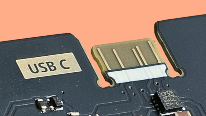
Sometimes when you’re making a PCB that you plan on programming over USB, but you only plan on plugging in a couple of times, it would be nice to make that connection without another BOM item. Over on GitHub [AnasMalas] has released a PCB edge USB-C connection symbol/footprint to do just that!
This isn’t the first PCB edge USB-C connector we’ve seen, but this one has some nice features. It’s available in both KiCad and EasyEDA formats, allowing you to easily add it into your preferred ECAD software. As well as supporting multiple software packages, there are two versions included: a 10-pin and 14-pin version. The 10-pin version has, on each side, 2 USB voltage pins, 2 ground pins, and a CC1 or CC2 pin on its respective side; this version is ideal if you’re looking to just supply power via the connector. The 14-pin version has all the pins of the 10-pin version with the addition of four data-positive and data-negative pins needed to relay information to the board, ideal if you’re planning on programming a microcontroller with this connection.
One important note is that, while most PCBs default to 1.6 mm thickness, if you use this connector you’ll need to drop that down to ~0.8 mm to properly interface with a common USB cable. [AnasMalas] also suggests using ENIG board finish to preserve the connectors on your USB cable.
For such a small and common connector, USB-C holds a ton of potential. Be sure to check out our series all about USB-C for more details.
Thanks to [Ben] for the tip.


If you only plan to use it a couple of times, why not use USART instead?
Because adding a USB/USART bridge IC would add complexity and BOM cost.
Back in the olden days the programmer chip was never part of the board. There were either holes or pads and that’s it.
You mean why not just keep doing whatever you’re already doing? Probably because that wouldn’t be news.
Like, imagine a hackaday article like: “Want to do a thing? People do the thing all the time and they still do it.”
Okay, yeah. So… maybe that actually is a fair percentage of the posts here. Nevermind.
A better idea is to leave a solder pad there, then you can solder on smaller 0.8mm circuit boards for the USB C interface.
Cheap enough and that way you don’t impact the existing PCB EMI by changing the thickness
I was thinking thickness as well. I’m a big fan of edge connectors, but are we really saving cost by going with a non standard board in order to save fifty cents on a connector?
Still, I usually put usb on all my boards and use it for power too, so I don’t see it as quite as “optional”. Though, since my boards tend to be general-purpose lego-style, I usually still include alternatives for alternate use cases. My go-to is usb-c and then break out vbus/gnd pins right next to it so I can power it either way.
That’s beautifully elegant. There’s something quite pleasing about just knowing the innards of any given device as attractive, or at least it offsets unpleasant aura “Oh god, hide it in an enclosure, I don’t care if I die in an electrical fire.”.
heh i’m not going to deny that it’s certainly an elegant solution, and an appropriate one for some use cases…but aesthetically when i look at i can’t stop seeing a lever arm and fracture point :) kind of funny how experience shapes our aesthetics.
maybe some through hole 0-ohm bridges with a little more distance to the board than usual?
FR-4 is awfully strong. More likely you’ll break your USB c cable’s connector.
You can snap FR4 pretty easily at 0.8 mm thickness.
especially if you compromise it with a few vias close to the smallest spot
Not at 0.8mm it ain’t. Plus your connector is metal-reinforced with its shielding.
I think this design is fun, but I’d be hesitant to put it anywhere accessible. Connected USB cables end up used as handles as often as not.
You have s strong point here! (pun intended)
Strong enough for an occasional debug or firmware update connector. After all, the ENIG gold plating is only good for around 100 cycles.
Regarding shapes.. I see balls.
See, I used my advanced mechanical design knowledge to add dog bone reliefs to make sure the dimensions are all correct and the connector is still well supported, we are not the same… (Just kidding… I immediately texted a group chat with a photo and captioned it “balls lol”)
I wonder if you could toughen up the part where the usbc tongue meets the board. Maybe on the bottom a an uncovered ground plate that you could fatten up with solder after the fact. Have it spread deeper into the main board to provide some strain relief maybe. Although it would still be weakest right where the usb cable ends.
if you plan to solder anything extra it may as well be a connector
Yes! You can add 0.2 or 0.3 mm of metal on either side where the silkscreen is, at that area the tongue is expected to be 1.2 mm thick, so use that to your advantage and extend that towards the board. It supports the cable better, too. Im trying to find something like that off the shelf and with adhesive
I did test snapping it, and yes, it is not that strong, but not the weakest either! If only I knew this would explode, I would’ve done a better job documenting everything. Thats on the way now!
I do mention on my twitter and LinkedIn post that you can make this way more rigid and supportive by adhering 0.2 or 0.3 mm of metal on either side of the connector, starting at the silk screen and extending into the board. The USB C paddle at that point is expected to be 1.2 mm thick, so we can use that to our advantage. In any case, use caution!
haha sorry i didn’t mean it as a criticism. You’re right on the money that it’s perfect for program / test…it’s not like your end users will leave it plugged in over night while they trip on the USB cable in the dark
Reducing the thickness and adding ENIG by itself may justify a new BOM item.
Very rare that I order a board without ENIG these days. And 0.8mm is obviously only suitable for certain applications where you would probably already be using that or something close.
Not everything has to be a one size fits all solution.
I do love raw PCB USB solutions. I will note, though, that upgrading to ENIG will almost always cost more than a BoM USB connector for the typical hobbyist board house order, so this isn’t the gimme solution for every project.
Good thing to lead with the “couple times” point to squash the inevitable rousing about how it won’t survive 1,000,000 insertions and other pointless HaD negativity.
When I was doing embedded design for aerospace systems, I needed a USB breakout for first-time configuration and RMA debugging. This was long before USB-C and the required PCB specs were too thick to pull this trick with mini/micro USB, and there was no open edge big enough for USB-A. I ended up putting pads at the edge where I could jam a mini header’s pins on them, but it wasn’t reliable so we ended up soldering a USB cable to the pads when needed.
Long story short, I would have loved this about 15 years ago!
Staggered holes and a right-angle 4 pin through-hole connector, with a separate (real) USB connector that you can share between projects. Staggered holes hold those guys surprisingly strong.
2nd the staggered hole suggestion. I’ve used this trick for ages for flashing bootloaders onto mcu’s just by shoving a six pin 0.1″ header (soldered to a ribbon attached to my programmer) into boards and then pulling the header out when done.
I’ve done the same with non staggered holes and just give the pins a little sideways tilt and light pressure when programming. Similar to pogo pins.
That’s actually a good point, though.In terms of resilience and reliability, you’re probably better off soldering a USB-A captive cable onto the board and having a full-size USB-A female jack on the other end.
You can secure it as firmly as you feel it needs (straps, S-channels, clamps, you name it) and if it ever goes bad it’s a cinch to replace. Assuming you can deal with USB 2.0, you’re only soldering 4 wires, or 9 if you have to have USB 3. (Or maybe 5/10? Do you need an extra shield wire, if you’re terminating a captive cable?)
If it’s only going to be used a few times, you might as well just put some test points and a couple alignment holes on the board. Then you can use pogo pins to connect to it and not have to use a thin PCB.
For this I use Tag-Connect’s TC2030-USB pogo pin USB cable. Then you only need testpoints / alignment holes on the PCB.
If you’re interested in other PCB edge connectors, here’s an HDMI one I designed:
https://forum.kicad.info/t/hdmi-pcb-edge-connector-for-raspberry-pi-pico-dvi-sock/48358/11
I did this with my business card a while back, it’s a very neat solution for things that aren’t gonna be used daily and repeatedly
Neat solution when board space is not a problem. That is not usually the case in my projects where I use a standard (to me) testpad layout, meanwhile the debug cable is just pogo pins attached onto a spring clip. Very reliable and takes almost no space on the PCB with the advantage that they can be later used with ATE if the board goes into mass production.
Hey Mat and others at Hackaday, thanks for sharing my library! I have updated the repo with some test results. Please have a look, thanks :)
Looking at pros and cons…
.
$0.5 on a million pcb’s are $500k.
There’s sometimes stricts dimensional constraints you have to stick to or the MCU needs to be debugged via USB.
You can use a 1mm or a 1,2mm and mill down to 0,8-0,6 from the other side of the PCB, not ideal but doable.
EMI can be an issue or not, depends on the project nature. I suppose that in case EMI could be an issue, the costs of the usb connector will be justified instead of the PCB design trickery.
Don’t just think about you. That’s just another tool in our toolbag. How we’ll use it or not it’s on us.
Anything has to be better than Micro-USB’s.