Part of setting up a microcontroller when writing a piece of firmware usually involves configuring its connections to the outside world. You define a mapping of physical pins to intenral peripherals to decide which is an input, output, analogue, or whatever other are available. In some cases though that choice isn’t available, and when you’ve used all the available output pins you’re done. But wait – can you use an input as an output? With [SCART VADER]’s lateral thinking, you can.
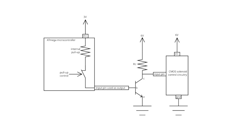
The whole thing takes advantage of the internal pull-up resistor that a microcontroller has among its internal kit of parts. Driving a transistor from an output pin usually requires a base resistor, so would it be possible to use the pullup as a base resistor? If the microcontroller can enable or disable the resistor on an input pin then yes it can, a transistor can be turned off and on with nary an output to be seen. In this case the chip is from ATmega parts bin so we’re not sure if the trick is possible on other manufacturers’ devices.
As part of our 2025 Component Abuse Challenge, this one embodies the finest principles of using a part in a way it was never intended to be used, and we love it. You’ve still got a few days to make an entry yourself at the time of writing this, so bring out your own hacks!


i don’t see the abuse. this looks like entirely normal use of a gpio.
Until someone forgets and set that pin to output and high, it will result in high current draw that can damage either the transistor or the AVR chip.
This should not happen: a) pullup is just enabled if pin is configured as input, b) yes, driving high now on output can damage pin!
Transistor holds the output voltage now at 0.8V… a high current for internal transistor. But often CMOS output pins are “safe” for an external short, limiting the max. current possible by its own resistance (but now burning power inside the chip)
With AVR the port register sets both the output state and the pull-up state. If the corresponding PORT register is set high, setting the DDR will result in either output high or input with pull-up.
So if you forget to disable the pull-up before switching to output, or you have the pin set up as output and you forget to change it to an input before you set the pull-up, the result will be output high and the transistor goes pop.
And the reason why you would want it to be an output is: when the transistor is supposed to be “off”, you want to set the pin to output low, so it isn’t left floating and able to trigger the transistor in error due to leakage or any stray currents such as from wires and PCB traces acting as antennas or inductors.
You don’t want the circuit to become an EMI detector by accident, so you need to drive the transistor base both low and high.
I took the article text to mean that the pin in question is a dedicated input.
In fact it’s further improved if the pull-up is enabled, OUT set to 0, and DDR used to toggle (assuming it’s a software bit-bang application). The base turns off much faster (orders of magnitude!) when current is withdrawn from it — BJTs are in fact voltage-mode devices, they just draw a convenient (sometimes..) base current to tell you when it’s on. ;-)
Sorry, what a nonsense. A pull-down would keep it a “real” input. An output driving low could be considered also as an input. The only way to use this “trick” (whis it is not) is just the fact, that pull-ups can only be enabled, when configured as input.
The pull-up can be very weak (e.g. 100K), so the transistor should be one with very low base current.
With MCU VDD 1V2 it might not work anymore.
BTW: a need to enable pull-up or not, and the actual input becomes floating when not enabled. This can cause an EMC issue: if input pin gets now a high voltage, e.g. due to electrostatic charge or leakage out of base from transistor – the MCU pin could be damaged.
Internal pull-ups is for avoiding inputs pins floating, not for driving external loads or acting as pull-up for open-drain logic.
No competent IC designer fails to protect a digital input with diodes.
“very low base current”. The current required to switch a small signal BJT is not fixed; it’s related to the collector current required to pull the collector near to ground. Using your 100k example and assuming a 5 V supply, about 43 uA would flow into the BJT base. For a BJT with a current gain of 100, the collector current could be as high 4.3 mA and still saturate. That allows Rc to be as low as 1.2 kohm, although good design practice would choose a higher value.
It’s not nice to be so picky to an amateur builder. This circuit is a hack presented on hackaday; using components outside the manufacturer’s intent is the very essence of this site.
Oops, the problem specifies an MCU voltage of 3V and the external voltage 6V. That changes the numbers to 23 uA, 2.3 mA, and 2.7 kohm.
Those are not idiot-proof. Keep hammering that protection diode and it will fail.
So?
“Internal pull-ups is for avoiding inputs pins floating, not for driving external loads or acting as pull-up for open-drain logic.”
Maybe try rereading the article, this was submitted for the component abuse challenge, you just proves that it does qualify.
Another “problem”: if no pullup enabled = input floating or even pullup enabled and transistor pulls now input to 0.8V… – putting the input pin voltage into “forbidden” voltage range… the internal input pin logic can now start to “oscillate”, trying to see a low or high, always toggling internal logic very fast. It can create a high current consumption, even burning so much current in internal input logic, that MCU (at least this pin) will get fried.
Technically, this input pin is floating or gets an input voltage level remaining in the transition zone (not low neither high, opening two transistors inside and creating a short current in internal logic). Both conditions (input floating and/or hanging somewhere in between) are not “allowed conditions”.
Just touching the input pin with your finger could damage the pin (or the ESD protection kicks in).
Or: the input pin will be “latched up”. So, it might work just once (and you have to power cycle the MCU).
BTW: why do you need this transistor?
If your solenoid control logic has a CMOS input – as to see in drawing, and as CMOS input not drawing “any” current…
Just toggle between pullup and pulldown. It will do the same job, but without any issues for MCU pin.
Just: a voltage translation to 6V does not seem to be CMOS.
You could also use an external pullup (but way larger as internal pulldown) and just toggle internal pull-down.
Use an external CMOS level shifter instead of transistor, at best one with Schmitt-trigger input and it works better.
I do not see really where the “strange” use case should be? This input pin could be also an open-drain output, acting also as an input pin. Just: as pullup you use internal pullup (just weak).
If open-drain drives low – it becomes an “input” (current flow) and input should read low.
The problem as stated does not specify that the MCU pin has pulldown capability.
The problem as stated does specify that the pin is “input only”.
The MCU datasheet will tell whether the BJT Vbe puts the input pin into the “undefined” range. For instance, the datasheet for ATmega328P specifies a low level on input pins to be no higher than 0.3xVcc, which is 0.9 V with a 3 V supply. Assuming a 2N3904 and the values from my corrected example above, Vbe will be below 0.5 V at 25 C and below 0.7 V at -40 C. Good enough for hobbyist work. If capacitively coupled noise turns out to be a problem, 100 pf to ground at the pin should attenuate any noise.
4000 series CMOS typically allowed supply voltages from 5 V to 15 V.
I’d be unhappy if this sort of circuit were used on commercial equipment that I paid money for, or that was in a life-critical application. OTOH, it’s just fine for having fun.
I’ve used a 3.3V pin on a PIC as a low output and changed it to an input to provide a 1.8V ‘output’ to the GPIO input on a 1.8V processor, with just one external component (pull up resistor to 1.8V) – saves adding a level shifter for a line that’s rarely changed (sets the processor into a programming mode)
Nice !
This trick results in lowest size C code blinky (that I am aware of) for stm32, which I recently uploaded to my GitHub repo as example delay_blinky_16 (28 bytes) :
https://github.com/rvl13/stm32-button-blinky-no-ram
This is how I handle I2C in my own code. I toggle between output now and input pulled high. It has always worked great for me without any external pull-ups
Years ago I wired the PIC12 MCLR pin as an output, but unfortunately it’s input-only, and the PCB was already made before I wrote a single line of code. I came to the same solution by just enabling the internal pull-up resistor.
Did something vaguely similar. GPIO connected to a button tied to VCC and to a set of variable resistors (a pot and an LDR+fixed-resistor) tied to ground. Set to output the GPIO provided power to the sensors (which were read via other pins) [sensors normally kept off to save battery power]. With the GPIO set to input the sensor resistors acted as pull-downs to ground, allowing the button state to be read.