Have you ever looked at a small development board like an Arduino or an ESP8266 board and thought you’d like one with just a few different features? Well, [Kai] has put out a fantastic guide on how to make an RP2040 dev board that’s all your own.
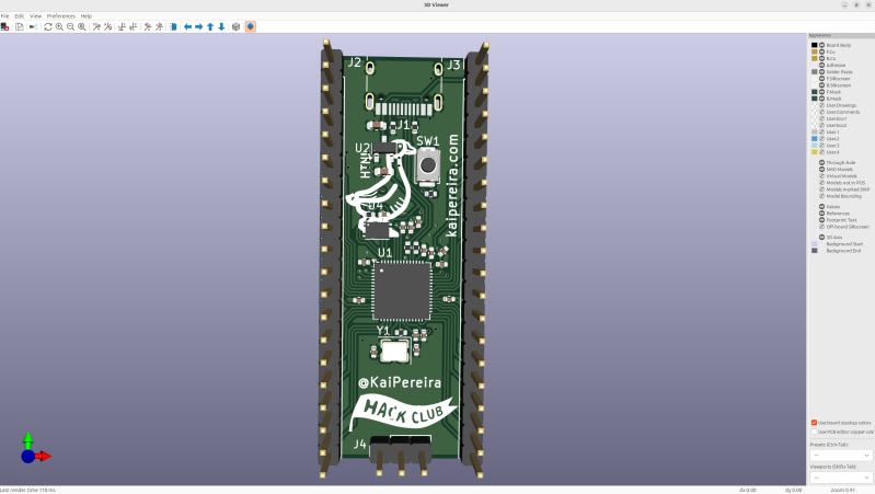
Development boards are super useful for prototyping a project, and some are quite simple, but there’s often some hidden complexity that needs to be considered before making your own. The RP2040 is a great chip to start your dev-board development journey, thanks to its excellent documentation and affordable components. [Kai] started this project using KiCad, which has all the features needed to go from schematics to final PCB Gerber files. In the write-up, [Kai] goes over how to implement USB-C in your design and how to add flash memory to your board, providing a place for your program to live. Once the crystal oscillator circuit is defined, decoupling capacitors added, and the GPIO pins you want to use are defined, it’s time to move to the PCB layout.
In the PCB design, it starts with an outside-in approach, first defining the board size, then adding the pins that sit along the edges of that board, followed by the USB connector, and then moving on to the internal components. Some components, such as the crystal oscillator, need to be placed near the RP2040 chip, and the same goes for some of the decoupling capacitors. There is a list of good practices around routing traces that [Kai] included for best results, which are useful to keep in mind once you have this many connections in a tight space. Not all traces are the same; for instance, the USB-C signal lines are a differential pair where it’s important that D+ and D- are close to the same length.
Finally, there is a walk-through on the steps needed to have your boards not only made at a board house but also assembled there if you choose to do so. Thanks [Kai] for taking the time to lay out the entire process for others to learn from; we look forward to seeing future dev-board designs. Be sure to check out some of our other awesome RP2040 projects.


The thing I always want on an ESP8266 board is an I2C bus for three or four devices. I never have enough I2C pins with a stock board, and wiring up a special I2C bus board introduces a new place for failures to occur.
Curious as to why?
Isn’t the point of an I2C bus that you can have multiple addressable devices on the same bus or do you have devices which talk the talk but don’t offer multiple addresses?
I think he just wants enough pins to do exactly that ie directly plug in multiple devices to the same i2c pins. It’s something you often need – I plug the esp8266/esp32 ‘dev’ board into a bigger board that does exactly that, but I can see why having it all on one board would be useful (though haven’t bothered to do it myself yet..).
You need lots of pins if you are plugging in lots of i2c devices…
Ah, that makes sense.
Personally I prefer a smaller dev board to maximise breadboard space so I can then breakout the pins I need to extra rows instead of having the extra board size used for stuff I don’t need (in that particular project) but that’s just my personal preference and I can see why others might want pins (though I have found the F-M or F-F jumper wires really unreliable after a few uses).
What I’d really like is a wider breadboard with an extra 2 or more holes per row…
BIG KUDOS to Kai for having written an article and not a freaking YouTube video!
And he is only 17!
I have hope for the future! :)
+1, great tutorial too!
I’m also impressed, I like youtube stuff but for an in depth like this, it’s really useful to have a comprehensive and well written article to follow.
I’ve found the hardest part of using the RP2040 is reflowing it successfully. I had one board out of 4 work where I could reliably see that the chip was functioning (seeing the 1v1 output from the 2040) but still could not successfully mount it. It’s a tough one to get right at home.
I’ve occasionally wondered why this chip has so many grounds compared to similar micros.
Provides good return paths, can be important for high speed signals or fast rising/falling times to decrease noise. Unsure if that’s super critical on the RP2040.
I don’t think the chip does, it has a big ground pad in the centre. The Pico has a lot of grounds, though.
Absolutely. I have managed to get the ‘comedy’ footprint successfully on a PCB, but it involves tinning the pad and using an oven. Where possible I now get someone else to put it on, which is more economical now JLCPCB will populate just 2 PCBs out of 5 instead of all 5. It was expensive when you get a PCB with 3 RP2040s on it wrong, it’s a bit cheaper now.
Super nice and inspiring! I would definitely add a couple TVS diodes, especially on the reset input. I’ve noticed that rpi pico bords are pretty sensitive to ESD.
Great posting. Building / copying / modifying an already existing product is a GREAT way to learn and practice the engineering steps, and gain some confidence. I recommend that any new engineer at a company take an existing product and fix / modify / add features to it. Then they will know the company processes, and are ready for the next step up.
There is a small flaw in the design. The BOOTSEL button resistor R6 needs to be as close as possible to the flash chip. It isn’t a place anywhere part as noted in the article. It is so the long PCB trace going to the button doesn’t affect the high frequency clock signal. It isn’t for current limiting.
This requirement is listed in the “Hardware design for RP2040” document not the RP2040 datasheet so easily missed.