In a recent video, [Andrew Zonenberg] takes us through the process of decapsulating a PIC12F683 to take a peek at its CMOS implementation.
This is a multipart series with five parts done and more to come. The PIC12F683 is an 8-pin flash-based, 8-bit microcontroller from Microchip. [Andrew] picked the PIC12F683 for decapsulation because back in 2011 it was the first microcontroller he broke read-protection on and he wanted to go back and revisit this chip, given particularly that his resources and skills had advanced in the intervening period.
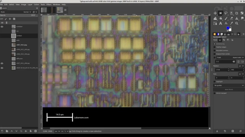
The five videos are a tour de force. He begins by taking a package cross section, then decapsulating and delayering. He collects high-resolution photos as he goes along. In the process, he takes some time to explain the dangers of working with acid and the risk mitigations he has in place. Then he does what he calls a “floorplan analysis” which takes stock of the entire chip before taking a close look at the SRAM implementation.
If you’re interested in decapsulating integrated circuits you might want to take a look at Laser Fault Injection, Now With Optional Decapping, A Particularly Festive Chip Decapping, or even read through the transcript of the Decapping Components Hack Chat With John McMaster.
Thanks to [Peter Monta] for the tip.


I used to work for a company that decapped chips to reverse engineer them. All the plants on the outside of the building near the fume hood exhaust were dead!
Take the safety precautions seriously!
One of the reasons I have scrubbers on my fume hoods instead of just venting untreated exhaust air outside.
They don’t even vent outside at all, in fact – it just goes through an activated carbon + alkali + HEPA filter stack the size of a minifridge door then recirculates the cleaned air back into the lab.
It’s good to be safe, but also an industrial application and a guy doing it one time for kicks in the garage are very different in scale
I’ve seen the failure analysis lab at a semiconductor fab, the speed with which they can decapsulate parts is frightening, from packaged device to clean die ready to mount for examination was literally under a minute.
There’s some seriously unpleasant, hot chemicals in use which destroy organic compounds so I’m not entirely surprised the local flora was unhappy
I’ve followed the series from the beginning, and sometimes follow along with Andrew’s Mastodon posts. Very cool stuff, and I love his home lab.
I second the precautions. Death by Hydrofluoric Acid is a terrible way to go. I’ve only had experienced scientists and engineers decap my chips for me in their well-equipped labs.
This guy sounds like a pro who knows how to deal with multiple metal layers, which I’m sure is finicky.
“….take a peak…” ?? peek
thanks!