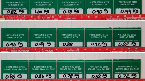
Most of us are familiar with the concept of producing PCBs in a panel, and snapping them apart afterwards. V-grooves that go most of the way through a PCB are one way to go about this, but a line of perforations along which to snap a tab is another. But what’s the best size and spacing of holes to use? Sparkfun’s [Nick Poole] spent some $400 on PCBs to get some solid answers by snapping each of them apart, and judging the results.
The nice thing about creating a perforation line (or “mouse bites”) is that drill hits are a very normal thing in PCB production, which makes creating this kind of breakaway tab a very straightforward and flexible method. However, it can be tricky to get results that are just right. Too sturdy, and breaking apart is a hassle. Too weak, and the board may break or twist before its time. On top of that, edges must also break cleanly. We’ve covered panelizing PCBs in this way before, but this is the first time we’ve seen someone seriously look into how to create optimal breakaway tabs.
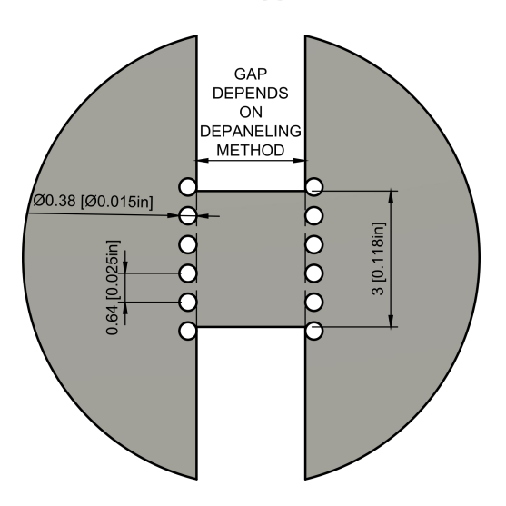
Data on designing mouse bites was sparse and a bit inconsistent, so [Nick] decided to figure it out empirically and share the results. The full details are available in Building a Better Mousebite (PDF download) but the essence of the recommendations are: 0.015″ unplated holes, spaced 0.025″ apart (center-to-center), tabs a maximum of 0.118″ wide (so as to be compatible with depanelizing tools), and holes that extend into the corners of the breakaway tab to avoid sharp edges. Holes should be placed slightly differently depending on whether one wishes to optimize the cosmetic appearance versus the physical smoothness of the board edge, but those numbers are the core of the guidelines.
To fine tune, [Nick] suggests increasing the spacing between holes to add strength, or just adding additional tabs. What about thickness of PCB? [Nick] tested boards both 0.8 mm and 1.6 mm thick, and while different amounts of torque were needed to snap the boards apart, things still worked as expected regardless of PCB thickness.
When it comes down to it, the best numbers will ultimately be the ones that your process or fab house can most efficiently handle, but [Nick]’s numbers should not steer anyone wrong, and it’s fantastic to see this kind of work go into refining such a common PCB feature.


