Sixteen wires of various colors are attached in pairs to record the electrical activity of split gill fungi (Schizophyllum commune) on a mossy, wooden stick. photo by Irina Petrova Adamatzky

Unconventional Computing Laboratory Grows Its Own Electronics

While some might say we’re living in a cyberpunk future already, one technology that’s conspicuously absent is wetware. The Unconventional Computing Laboratory is working to change that.

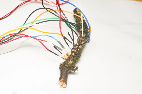
Previous work with slime molds has shown useful for spatial and network optimization, but mycelial networks add the feature of electrical spikes similar to those found in neurons, opening up the possibility of digital computing applications. While the work is still in its early stages, the researchers have already shown how to create logic gates with these fantastic fungi.

Long-term, lead researcher [Andrew Adamatzky] says, “We can say I’m planning to make a brain from mushrooms.” That goal is quite awhile away, but using wetware to build low power, self-repairing fungi devices of lower complexity seems like it might not be too far away. We think this might be applicable to environmental sensing applications since biological systems are likely to be sensitive to many of the same contaminants we humans care about.

We’ve seen a other efforts in myceliotronics, including biodegradable PCB substrates and attempts to send sensor signals through a mycelial network.

Via Tom’s Hardware.

A notated illustration showing how a mycelial network may be functionalized as a PCB substrate. The process starts with Cu vapor deposition onto the network followed by Au either by more vapor deposition or electrodeposition. Traces are then cut via laser ablation.

MycelioTronics: Biodegradable Electronics Substrates From Fungi

E-waste is one of the main unfortunate consequences of the widespread adoption of electronic devices, and there are various efforts to stem the flow of this pernicious trash. One new approach from researchers at the Johannes Kepler University in Austria is to replace the substrate in electronics with a material made from mycelium skins.

Maintaining performance of ICs and other electronic components in a device while making them biodegradable or recyclable has proved difficult so far. The substrate is the second largest contributor (~37% by weight) to the e-waste equation, so replacing it with a more biodegradable solution would still be a major step toward a circular economy.

To functionalize the mycelial network as a PCB substrate, the network is subjected to Physical Vapor Deposition of copper followed by deposition of gold either by more PVD or electrodeposition. Traces are then cut via laser ablation. The resulting substrate is flexible and can withstand over 2000 bending cycles, which may prove useful in flexible electronics applications.

If you’re looking for more fun with fungi, check out these mycelia bricks, this fungus sound absorber, or this mycellium-inspired mesh network.