A notated illustration showing how a mycelial network may be functionalized as a PCB substrate. The process starts with Cu vapor deposition onto the network followed by Au either by more vapor deposition or electrodeposition. Traces are then cut via laser ablation.

MycelioTronics: Biodegradable Electronics Substrates From Fungi

E-waste is one of the main unfortunate consequences of the widespread adoption of electronic devices, and there are various efforts to stem the flow of this pernicious trash. One new approach from researchers at the Johannes Kepler University in Austria is to replace the substrate in electronics with a material made from mycelium skins.

Maintaining performance of ICs and other electronic components in a device while making them biodegradable or recyclable has proved difficult so far. The substrate is the second largest contributor (~37% by weight) to the e-waste equation, so replacing it with a more biodegradable solution would still be a major step toward a circular economy.

To functionalize the mycelial network as a PCB substrate, the network is subjected to Physical Vapor Deposition of copper followed by deposition of gold either by more PVD or electrodeposition. Traces are then cut via laser ablation. The resulting substrate is flexible and can withstand over 2000 bending cycles, which may prove useful in flexible electronics applications.

If you’re looking for more fun with fungi, check out these mycelia bricks, this fungus sound absorber, or this mycellium-inspired mesh network.

Rubber Stamping Your Way To Custom PCBs

Many of us now outsource PCB production to board houses overseas, which offer high-quality boards with increasingly impressive turnaround times. You might still brew up your own PCB, though, and a reader found this great old hack from [William Hare] that might be worth a look.

Forget toner transfer or marker pens — this build is all about speed. [William] decided to use a rubber stamp to quickly transfer ink to a copper board that can then be etched to produce a PCB. It’s simple and straightforward enough. We’ve used the same technique for silkscreen and pad art, but never as an etch resist.

The trick is to make several rubber stamps with different circuit elements, though. The genius part is that you can then assemble a PCB by simply stamping down the various circuit components you need. The boards will still need to be drilled if you’re working with through-hole parts, but tipster [Shri] notes that the technique is super useful for producing single-sided surface mount boards.

We’ve seen some other unique methods to producing PCBs at home, such as using a 3D printer to help out. If you’ve got your own innovative homebrew PCB hacks, be sure to drop us a line!

Thanks [Shri Hari Ram] for the tip!

Hackaday Links Column Banner

Hackaday Links: November 1, 2020

We normally chuckle at high-profile auctions where people compete to pay as much as possible for items they clearly don’t need. It’s easy to laugh when the items on the block are things like paint-spattered canvases, but every once in a while some genuine bit of history that really piques our interest goes on sale. Such is the case with what is claimed to be an original Steve Wozniak-built Blue Box, going on sale November 5. The prospectus has an excellent summary of the history of the “Two Steves” and their early business venture making and selling these devices to Berkeley students eager to make free long distance phone calls. The item on sale is a very early rev, most likely assembled by Woz himself. The current owner claims to have bought it from Woz himself in the summer of 1972 while on a roadtrip from Sunnyvale to Los Angeles. Estimated to go for $4,000 to $6,000, we really hope this ends up in a museum somewhere — while we’ve seen attempts to recreate Woz’s Blue Box on Hackaday.io, letting a museum study an original would be a great glimpse into our shared technological history.

Not in the market for old tech? No problem — Digilent wants to get rid of 3,000 PCBs, and quickly. They posted the unusual offer on reddit a couple of days ago; it seems they have a huge stock of populated boards for a product that didn’t quite take the market by storm. Their intention is likely not to flood the market with scopes cobbled together from these boards, but rather to make them available to someone doing some kind of art installation or for educational purposes. It’s a nice gesture, and a decent attempt to keep these out of the e-waste stream, so check it out if you have a need.

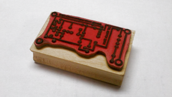
Speaking of PCBs, SparkFun has just launched an interesting new service: SparkFun À La Carte. The idea is to make it really easy to design and build prototype boards. Instead of using traditional EDA software, users select different blocks from a menu. Select your processor, add components like displays and sensors, and figure out how you want to power it, and SparkFun will do the rest, delivering a fully assembled board in a few weeks. It certainly stands to suck the fun out of the design process while also hoovering up your pocketbook: “A $949 design fee will be applied to all initial orders of a design”. You can get your hands on the design files, but that comes with an extra fee: “they can be purchased separately for $150 by filling out this form”. But for someone who just needs to hammer out a quick design and get on with the next job, this could be a valuable tool.

Another day, another IoT ghost: Reciva Radio is shutting down its internet radio service. A large banner at the top of the page warns that the “website will be withdrawn” on January 31, 2021, but functionality on the site already appears limited. Users of the service are also reporting that their Reciva-compatible radios are refusing to stream content, apparently because they can’t download anything from the service’s back end. This probably doesn’t have a huge impact — I’d never heard of Reciva before — but it makes me look at the Squeezebox radio we’ve got in the kitchen and wonder how long for the world that thing is. It’s not all bad news, though — owners of the bricked radios will now have a great opportunity to hack them back into usefulness.

By the time this article is published, Halloween will be history and the hordes of cosplaying candy-grubbers who served as welcome if ironic respite from this non-stop horror show of a year will be gone. Luckily, though, if it should come to pass that the dead rise from their graves — it’s still 2020, after all — we’ll know exactly how to defeat them with this zombie invasion calculator. You may remember that last year Dominik Czernia did something similar, albeit with vampires. Switching things up from the hemophagic to the cerebrophagic this year, his calculator lets you model different parameters, like undead conversion percentage, zombie demographics, and attack speed. You’ve also got tools for modeling the response of the living to the outbreak, to see how best to fight back. Spoiler alert: everyone will need to bring Tallahassee-level badassery if we’re going to get through this.

Component Shelf Life: How To Use All That Old Junk

There are two types of Hackaday readers: those that have a huge stock of parts they’ve collected over the years (in other words, an enormous pile of junk) and those that will have one a couple of decades from now. It’s easy to end up with a lot of stuff, especially items that you’re likely to use in more than one design; the price breakpoints at quantities of 10 or 100 of something can be pretty tempting, and having a personal stock definitely speeds the hacking process now that local parts shops have gone the way of the dinosaur. This isn’t a perfect solution, though, because some components do have shelf-lives, and will degrade in some way or another over time.

If your stash includes older electronic components, you may find that they haven’t aged well, but sometimes this can be fixed. Let’s have a look at shelf life of common parts, how it can be extended, and what you can do if they need a bit of rejuvenation.

Continue reading “Component Shelf Life: How To Use All That Old Junk”

The Components Are INSIDE The Circuit Board

Through-hole assembly means bending leads on components and putting the leads through holes in the circuit board, then soldering them in place, and trimming the wires. That took up too much space and assembly time and labor, so the next step was surface mount, in which components are placed on top of the circuit board and then solder paste melts and solders the parts together. This made assembly much faster and cheaper and smaller.

Now we have embedded components, where in order to save even more, the components are embedded inside the circuit board itself. While this is not yet a technology that is available (or probably even desirable) for the Hackaday community, reading about it made my “holy cow!” hairs tingle, so here’s more on a new technology that has recently reached an availability level that more and more companies are finding acceptable, and a bit on some usable design techniques for saving space and components.

Continue reading “The Components Are INSIDE The Circuit Board”

How To Take Pictures Of PCBs

While we’ve covered light box builds and other DIY photography solutions, general picture-snapping tips and tricks are a bit out of the purview of what we normally write about. Nevertheless, [Alain] just put up a great tutorial for taking pictures of PCBs. This is a great skill to have — no one cares about what you’ve built unless you have a picture of it — and the same techniques can be applied to other small bits and bobs of electronic equipment.

As with all matters of photography, light is important. [Alain] built a DIY light box using two cheap outdoor square LED panels and some scrap wood. There’s really nothing to this build: just build a box that holds soft, diffused light.

A camera is a little more complicated than a box, and here [Alain] is using an entry-level DSLR with a kit lens. The takeaway here is to set the aperture to the highest number (or smallest hole) possible while still keeping a reasonable shutter speed. This increases the depth of field and produces a picture where the board and the tops of components are in focus.

There are a few more tips for getting the best PCB pics possible including shooting in RAW for Aperture or Lightroom, getting a macro lens, and using a tripod. Like all things, there’s a law of diminishing returns, and even with a smartphone camera and a DIY light box, you can produce some fantastic pics of PCBs.

Use All That Extra Space With PCB Panelization

Anyone who’s made a PCB has encountered the conundrum of having to pay for space that you don’t use… for instance, designing a round PCB and seeing the corners go to waste. The solution? Smaller boards added to the blank spots.

One logical stumbling block might be that you simply don’t have a small PCB design ready to go. Latvian hacker [Arsenijs] created a resource of small PCBs that can be dropped into those blank spots, as well as a tutorial on how to combine the gerbers into a single panel.

Great minds think alike, and this guide is following hot on the heels of [Brian Benchoff’s] article on panelization. They’re both a great read. It’s interesting to think that not long ago we would see multiple guides on home etching boards and now we’ve climbed the production ladder to guides that help better utilize PCB fab houses. Neat!

This project seems a logical spinoff of [Arsenijs]’s ZeroPhone Pi smartphone project, a finalist for the 2017 Hackaday Prize that makes a low-cost phone using a stack of PCBs. One imagines that while prototyping the phone [Arsenijs] ended up with a lot of wasted space! Fill that up with smaller designs like breakouts, or decorative items like a hackerspace business card. If you’re looking for small PCBs you can find a few in the files area of the project on Hackaday.io. Otherwise, you can share yours and [Arsenijs] will add them.