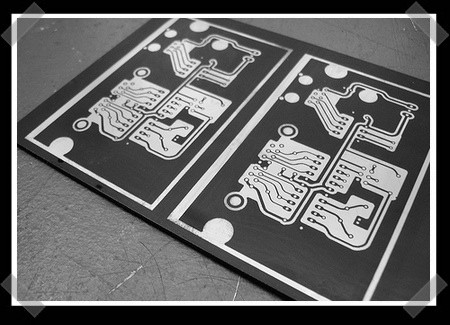
While we hope you enjoyed our How-To: Etch a printed circuit board, toner transfer certainly isn’t the only way to get the job done. [Garrett] from macetech has recently been playing around with using an Epilog laser to etch PCBs. He started by applying a thin even coat of flat black spray paint to the copper board. The laser is used to remove paint in areas that you want the copper removed. Once that’s done, you proceed with etching as usual. He eventually removed the paint mask using acetone. The result has very fine, sharp traces, but most people that have tried this agree that using spray paint is less than ideal.


23 thoughts on “Laser Etching Printed Circuit Boards”
Leave a Reply
Please be kind and respectful to help make the comments section excellent. (Comment Policy)


Maybe using layout fluid would work better. It’s designed to put a thin even film on metal which you then scribe into to mark cut lines. It typically has a complementing remover liquid that takes it off.
IF it stands up to the etch process I think it would be ideal.
I’m pretty sure you can just “etch” the photo negative right on the board. The laser will vaporize the copper. You’ll need to play around with the power settings though, and it’s probably not the fastest way to do things. Hell you could probably raster cut the edges if you want to do multiples.
or maybe wax which you could remove in boiling water?
you can do it directly, you just need to crank up the power. LPKF makes laser systems that do just that: http://www.lpkfusa.com/protomat/pl_s.htm
The catch is that the systems cost 150k+
Yeah, the Epilogs can’t burn away copper. Also, I found the flat black spray paint to be as close to ideal as I can imagine. You could see the pixel corners from the 600DPI file I used, even higher resolution is possible. Maybe I just happened onto some paint that works especially well.
So, I have done this with a laser cutter, and am finding that the flat black spray paint that I am using simply is not good enough. When it is ablated by the laser, it has a tendency to redeposit on the copper surface, and must then be removed using some chemical that also has a tendency to remove the paint which you don’t want gone.
Unless I find something better than flat black spray paint, I am convinced that the PressNPeel method is easier.
The upside to this technique is that you are able to create smaller features with the laser cutter than you can with the PressNPeel technique.
Maybe the laser could activate the resist on a photosensitive board? Usually that photoresist is UV sensitive, and I don’t imagine the epilog uses a UV laser, but maybe you could experiment with longer exposures to the laser. You’ll want to keep your environment otherwise dark when you’re doing this, because room lighting will eventually expose the whole board.
I found photoresist to not be difficult to expose; when I used it, I used a household compact fluorescent light bulb, and it only took a few minutes to fully expose the board.
re. laser activation of resist:- see my article on using an HD-DVD laser diode to expose resist :)
-A
@7: the magical chemical i’m using is 99% rubbing alcohol from safeway on a paper towel. It takes off the residue without destroying the resist pattern. Oh, and the paint I’m using is Rust-Oleum “Painter’s Touch” flat black from Home Depot. I go ahead and wipe the copper clad with alcohol before spraying it, though I don’t know if it really matters. I’m using a 45 watt Epilog laser at 100 speed and 50% power, 600DPI. That’s a little more power than they recommend for painted brass, I wanted to make sure the paint was really vaporized off the surface.
The main thing I like about this method is the reliability. Whatever you put in your PCB absolutely will appear in your resist pattern. Press-n-peel or laser toner transfer, you may not get everything down. With toner transfer on magazine paper, you even have to scrub all the fibers out of the ink. Sometimes I’d spend 15 minutes carefully scrubbing a board and then finally a few IC pads would fall off.
Getting the pattern onto the board requires one overnight drying step, and then 5 minutes laser time, but the pattern will absolutely make it onto the PCB and then very little preparation before etching.
I’m going to do some more experiments; double-sided boards, spraying paint on an etched board and then lasering off the pads to make soldermask, I even have an idea for silkscreen. Lots of fun….
Absolutely.
we did this in high school in 2000, we used a thick blue paint from our graphics department, and etched off the paint using a negative of the circuit with our wood shop department’s etching laser.
as for garrett’s response, we also did screen printing before we lasered the boards. i think (i’m not sure, i wasn’t involved wit h this process) they printed out the patterns on transparency’s and transfered them onto the light sensitive green stuff (emulsion? it’s been awhile) but that wasn’t very good for tight boards. some of the paint would smear over and connect tracks. so in the end we did it all with lasers as part of our high school tech-ed class.
Brandon- I also run a 45w Epilog and there is a setting in the driver that lets you do bottom-up engraving. That prevents the redeposit as the laser starts at the bottom of the board and works towards the top with the airflow direction instead of against it. I don’t know which other lasers offer that in the driver though. Makes a huge difference in engraving two-colored plastics.
Pretty cool!
Check out this place, http://www.etchingpros.com, they do laser etching – on marble slabs up to 4 x 8 feet! Now that’s a serious laser!
0013 400019331 000421 EACH 1
BOARD , PRINTED CIRCUIT: FUNCTION: UV
EPROM; ADDITIONAL DATA: UV
EPROM,M27C1001-10F1 128KX8BI 1MB, TS
STOCK NO. 169-3439, MFR: ST
ELECTRONICS, MFR PART NUMBER:
M27C1001-10F1 FDIP32W, USED FOR MARK V
CARDS. FOR GE GAS TURBINE INSTALLED IN
ASIR POWER STATION. GENERAL
ELECTRIC/DIELEKTROL/LENTRONICS P/N#
M27C1001-10F1 ST ELECTRONIC P/N#
M27C1001-10F1 APPLICATION:
MFR NAME:REFER TO MFR ON LINE 500
MFR P/N :M27C1001-10F1
Bid Number Bid Send Bid Close
Q090690252415L 02/06/2009 16/06/2009
0005 203647889 000260 EACH 1
BOARD , PRINTED CIRCUIT: FUNCTION:
EARTH FAULT DETECTION; ADDITIONAL DATA:
APPLIC:FOR BATTERY CHARGER; TYPE:
125TPR100; CODE: A6873-010P0T1; VOLTAGE
RATING : 125 VDC; CURRENT RATING : 100
A; SAFT NIFE P/N# B00625400300
Bid Number Bid Send Bid Close
Q090589781255L 02/06/2009 10/06/2009
0007 203647889 000260 EACH 1
BOARD , PRINTED CIRCUIT: FUNCTION:
EARTH FAULT DETECTION; ADDITIONAL DATA:
APPLIC:FOR BATTERY CHARGER; TYPE:
125TPR100; CODE: A6873-010P0T1; VOLTAGE
RATING : 125 VDC; CURRENT RATING : 100
A; SAFT NIFE P/N# B00625400300
Bid Number Bid Send Bid Close
Q090589781255L 02/06/2009 10/06/2009
Very interesting. I may try this for SMT stencils. I usually send PCB’s out, but I’ve been looking for a good solution for cheap solder paste stencils.
I have an old and crotchety Epilog Summit that still does 10W or so. I’ve tried making stencils in drafting mylar, but the power setting is just too touchy, there is a fine line between getting a clean cut and getting goo.
The best material I’ve found so far is 17lb drafting velum, which makes a decent 2 or 3 use stencil. 0.8mm lead pitch TQFPs are almost doable but not reliable, and I’ve not had good luck with anything finer pitch. Works great for SO parts and 0603, etc.
So I’m thinking I’ll try your trick, but use 0.003″ brass sheet metal. That should make a decent stencil.
-dave
I tried the following:
120W etching laser
20% power
25% speed
500 ppi
Wiped board with 91% isopropyl alcohol before painting with rust-o-leum flat black (24 hr dry time). Etched paint off. Removed paint splatter from pattern with a light rub with alcohol. Be careful, too much pressure will remove all the paint. Bathed in Radio Shack Ferric Chloride for 18 minutes, agitating the whole time. Removed remaining paint with alcohol, scrubbing hard.
Results were amazing. I tested traces as small as .3 mm and they came out perfectly. This method is the best I have ever seen. If you can get your hands on an etching laser (try your local university), I highly recommend it.
Thank you for thinking of me!
Update for the 5 people following this hack. Using the same 120W laser I was able to make vias with 100% power and 1% speed. I only had time for one test so far but it seemed to burn all the way through leaving some copper connecting the two sides. I easily unshorted them with a sharp utensil but it would be interesting to see if 120W could really do the trick.
Dave: Put wet paper under the mylar in your laser. You can cut 0.5 mm SMD pads with this method. The power setting is much less finicky. I think I do 100% power, 50% speed, 5000 Hz, on a 45 or 60 watt Epilog, but I didn’t fine-tune this because it worked the first time.
Chris
I think I have figured it out…Making laser PCBs.
To begin with I make the art work on Corel Draw 5X, then I copy all of the art work to two new layers, One is positive one is negitive. The positive one is of the copper I want to remove, the negitive one is of the traces and pads.
The real key is the ability to place the PCB in the exact same place in the laser. I made a jig to hold my PCB and don’t do ANY lasering on the jig, only in the center of the jig which is hollow.
So I first mount pcb in jig after painting and drying for 24 hours. Then laser the paint where the copper is to be removed. Etch the board, rinse, dry. Remount the board, laser the traces and pads and it is finished. Drill the holes for non surface mount parts.
I’ve been doing this for a few years now. I use any spray i can find. White automotive undercoat seems to work well and has a good contrast with the copper.
I use pcb wizard to produce the circuit design. I export this as a wmf file and import this into techsoft 2D design.
It needs flipping and reducing in size by 5%.
Then with the laser, we have a 30w model, i set it to raster the negative. Full power at 40% speed.
I can do a 300 x 200mm board in 20 mins.
Then i spray it with kitchen cleaner oven cleaner also works but can act as paint stripper. This gets rid of paint residue.
Then into etch tank. Our new toy is a roto etcher. Finished in under 3 mins.
Then rinse, drill holes, remove paint on tracks.
Much cheaper and less time critical than UV boxes, masks, developing etc etc.
Chris pryor
I’ve been developing (and duplicating mostly) this method and have found a few process improvements that I wanted to share…my process that yield beautiful results with much less mess and includes solder mask looks like this:
1, Spray copper clad board with rustoleum flat black high temp grill paint aerosol
2. Tape to a stiff and flat removable fixture (I use pins in my CO2 laser)
3. Laser etch paint. 1 pass, 10mA output current. Be sure to be at the optimal (smallest diameter) focal length.
4. Clean board with a toothbrush or other scrubbing brush with a baking soda-water mix. It should only take a few seconds of scrubbing to get the soot off the copper
5. Chemical etch
6. Dip into baking soda-water bath to neutralize acid
7. Allow to dry and paint again with the grill paint
8. Fixture in laser and etch away solder mask pads
9. Brush with baking soda again
*Advantages here are that the grill paint is high temp, so unless your PCB gets over 1200 dF you don’t need to remove the resist, and the grill paint works well as a solder mask as well. The grill paint says silicone base on the can…I’m assuming its safe to laser etch.
**I’m working to find a tape that could substitute for the black paint without the need to clean afterwards or wait for paint to dry. So far I haven’t found a tape that cleans up well after laser etching, so the grill paint is the best I’ve found.
Hope it helps someone,
Jared