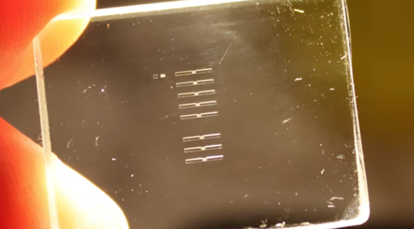
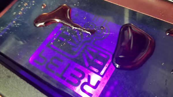
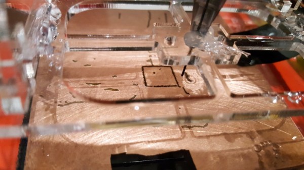
These days, PCB fab houses are just about everywhere, and you can’t go buy a taco without walking past eight of them. Still, some out there still like to etch their PCBs at home. If that sounds like you, you might see some value in [Chris Borge]’s PCB agitator.
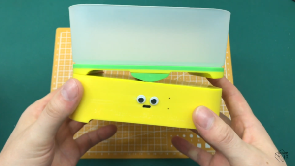
The design mostly relies on 3D printed parts, including the main body. It has a heavy base which is filled with concrete to keep it nicely weighed down on the table. A table for holding a PCB and fluid tank is then installed on top, via a bearing which allows it to pivot in one axis. An Arduino Nano commands the agitation of the table top, and hence the PCB etching tank, with a servo used to actually shift the table back and forth.
It’s a simple design — far simpler than some of the advanced coffee-making hardware we’ve seen recently. Regardless, it gets the job done, and done well! In testing, it accelerated [Chris]’s etching jobs significantly, we’re talking hours here. Meanwhile, if you don’t have a 3D printer on hand, you could always try building one out of junk instead!