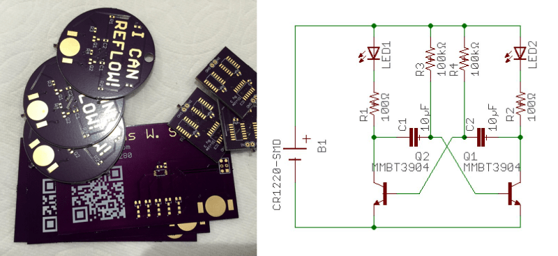
[Nick Sayer] can reflow, and he can prove it. He designed a simple blinking-LED circuit that uses SMD parts to, well, blink LEDs. That’s not the point, though. It’s designed to be a test platform for reflow soldering, and to use a minimum number of valuable parts. Plus, it says “I can reflow!” in exposed copper. What else do you want?
OK, as far as “proving it” goes, the badge isn’t 100% reliable — we hand-solder 0805 components all day long. But still, if you want to try your hand at reflowing a circuit board, and you don’t want to ruin a lot of expensive parts if you fail, something like this is a good idea.
The design is open, and it’s really the idea that’s the point here anyway. How about something that would be really onerous to hand-solder, but still cheap? We’re thinking a matrix of tiny LEDs and a shift register or something.
We just ran an article on a hand-soldering challenge board, this seems the perfect complement. Display both proudly on your desk and confound and amaze your coworkers!


Why would anyone bother with some special badge, when there are tons of old PCBs full of SMD goodies? Just desolder them, reflow, and test with multimeter for shorts or bad joints…
They’re a good draw for Makerfaire booths or hackerspace lesson nights.
If you’ve never thought about SMD parts before you may not realize their potential & a cheap board is a great way to draw the interest of the uninitiated.
There are makerfaire robot blinken badges that will draw more people than a booth can reasonable teach during a 4h makerfaire, this is the next step up from that.
What inspired me was that there are lots of “I can solder” badges that are similar, but use through-hole parts. I searched and couldn’t find any equivalents for SMD. So I designed one myself.
I think its an awesome idea, i have done some slight reflow but nothing too crazy so this would be a nice test board. Definitely ordering a pack!
Story time.
Back when I was a teenager in the 80s, I did a lot of Heathkits. I tried to make my own single-sided PCB with a copper clad board, a resist pen, that nasty brown etchant, and the smallest drill bit I could get. Even with a drill press, I couldn’t get the holes lined up well enough for a DIP. I had no way to align a double-sided design and wouldn’t have been able to do through-plated vias, soldermask, silk screen… And then towards the end of the decade, I saw surface mount beginning to dominate consumer electronics and felt at the time that that was the death knell for hobbyist electronic design. So I steered towards a career in software. I still remained somewhat current with hardware – mostly via ham radio – but it wasn’t primary. I experimented with some early 68HC11 and Basic Stamp stuff, but… meh…
Fast forward to 3 years ago. I leased an electric car and got an EVSE for it from Home Depot for $700. It astonished me that what amounted to a fancy power switch was so expensive, so I had to figure out what was inside. That got me in touch with the OpenEVSE project, which in turn lead me to discover Arduino, and then OSHPark, and EAGLE… and just like that, all the stuff in my youth that told me that it wasn’t going to be possible for hobbyists to do good hardware vanished.
I made an EVSE testing gizmo (when one of your hobbies is building EVSEs, you know you’ve taken a weird turn) based on an ATTiny85. It was a through-hole board, and I decided to see if I was wrong – that it was actually possible to make a surface mount version of it. So I designed a board for an SMD version of the same device and then ordered the parts. I’m embarrassed to say that that order consisted of multiple cut-tapes of single parts. The pickers at DigiKey must have been either laughing hysterically or cursing. I took the board and parts to the lab at the office that had a fine tipped soldering iron and a microscope station and sat down to put it all together. I did get it working, but it took me two hours – easily 10 times longer than the through-hole version. I wrote about this experience on the OpenEVSE mailing list and Chris Howell – the head of that project – replied (not quoting literally here), “oh, no, that’s not how you do SMD. You should use reflow!”
So that little vocabulary word fueled a bunch of research and I converted a toaster oven into a reflow oven (I sell that conversion kit on Tindie now) and haven’t looked back.
The first time I tried to apply solder paste and do PnP with tweezers, it looked like a disaster when I was done. I looked at it and thought to myself that there was no way this was going to work. For a brief moment, I almost picked it up and threw it in the trash, but something stopped me and told me to at least try the reflow oven out.
So I put the board in and pressed ‘start’ on the oven controller and waited.
When it was done, I pulled it out and my jaw hit the floor. The board looked like it had been manufactured by a factory in Shenzhen. I learned that solder mask and surface tension are the magic that make results like that happen.
Last year (2015) at Maker Faire, I took my reflow oven and was making little blinky earrings, demonstrating hobbyist PnP and reflow. I dunno, somehow that didn’t resonate with the crowd as much as I had hoped it would.