Making a PCB is very simple; it does not consume a lot of time and the results look professional. After reading this How-To and watching the step by step video, you will be able to make your own PCB in your workshop using just a few inexpensive materials.
Many people use protoboard and point-to-point wire everything, but needing multiple copies of the same circuit is the reason that forces many away from using protoboard. After making your first circuit board, you might not point-to-point wire anything again!
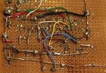
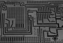
For your first circuit board, one goal is to keep the circuit single sided so you can etch using single sided copper clad. This will allow you to gain some experience before moving on to double-sided. If you need topside traces, simply run a few jumper wires on the top. There are many complete circuit layouts you could try like the Hack a Day design challenge winner.
Here is a list of materials you will need to produce a single-sided board. With the exception of the copper clad and PCB drills, everything on this list is easily obtained at your local store.
Materials: Muratic acid, common household hydrogen peroxide, safety goggles, good quality magazine pages (cut to 8×11), laser printer, single sided 1 ounce copper clad, a plastic container the board will fit in, soft plastic brush, clothes iron, lacquer thinner, rubber gloves, paper towel, tin snips, drill or rotary tool, PCB drill bits, Scotch Brite scrubbing pad, good ventilation, 5-gallon plastic pail full of water.
Now, here is how you do it:
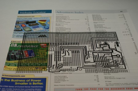
Print the bottom side layer on a piece of paper from a high quality magazine. Use one actual page from the magazine, the thicker and shinier the magazine paper the better, but do not use the cover. You must use a laser printer, not an inkjet. If your printer uses ink cartridges and not toner cartridges, it will not work. If you do not have a laser printer, you can work around this by printing to white paper and using a photocopier set to the darkest setting to copy the layout to the magazine paper. If the paper jams in the printer, you are not using a thick-enough magazine page. Again, do not use the magazine covers, as they do not work.
Magazine pages are used because they work well, and they are cheap! The reason they work is because the paper is very glossy and the toner does not adhere well to the glossy pages. The printing used on the magazine page is ink and it does not come off, but toner does. Toner is actually a plastic polymer, and different toners may yield varied results. In our experience, a genuine HP toner cartridge was used with great success; an Office Max brand yielded poor results. The sole purpose of the toner is the protect the copper below it from etching away, you only want the uncovered areas to etch.
Next, wash your hands to remove any oils. Keep handling to a minimum once the pages are printed and do not touch the laser printing with your fingers; this could get oils on the printing. Keep pages as flat as possible.
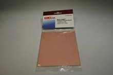
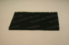
Very carefully, remove the copper clad from the packaging. Do not touch the copper surface for the same reason as above. You can cut the copper clad to size using a tin snip if needed. Use the Scotch Brite scrubbing pad to gently buff the surface (Scotch Brite is a popular brand of of plastic scrubbing pad meant to emulate steel wool). Do not use steel wool because it will embed steel into the copper. Clean off the residual dust with a slightly damp paper towel.
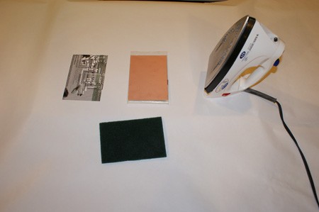
Find a hard, very flat, sturdy, heat resistant surface. Empty the water out of the clothes iron and set the iron on the hottest setting. Allow the iron to get hot.

This is both side of a piece of copper clad. Place the blank side facing down and copper side facing up. Align printing/paper onto copper clad board with the printing facing the copper. Do not allow it to move.
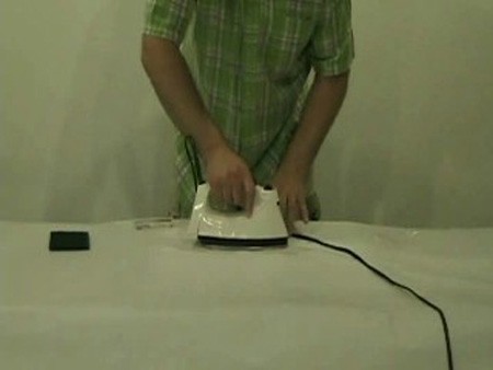
Firmly press the iron onto the back of the magazine paper, sandwiching it between the copper clad and the iron. Pressing hard without moving the iron, hold the iron perfectly still for one full minute. Do not move the iron at all during this minute, and push hard, really hard!
Then, for four more minutes, slowly move the iron around making sure to put a lot of pressure on the paper, but not allowing the paper to slide on the copper. When done, let the board fully cool before you move it at all. This will allow the toner to adhere to the copper and prevent you from being burned.
Put the board in cold water and let soak for five minutes. After five minutes, try to peel the wet paper from the board leaving only the toner/print from your laser printer. Only the toner should be left adhering to the copper. If the paper does not come off easily, let it soak in the water for a while longer. If necessary, rub with your finger to remove any paper, leaving only the toner. It’s ok if there are a few excess paper fibers stuck to the toner.

If you find not every trace adhered to the copper clad or it is misaligned, use lacquer thinner and paper towel to clean the toner from the copper board and start over. If the traces look good then move on. Inspect the traces carefully, however, because what you see now will be your finished product.
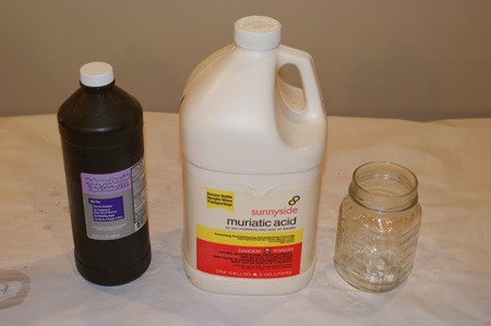
In a well-ventilated area with a fan, add 2-cups hydrogen peroxide to a plastic container. Gently pour in 1-cup Muriatic acid, to create the etching solution. Always wear goggles, gloves, and do not inhale the fumes. Do not use any metal containers, measuring cups, stainless steel sinks, or tools with this mixture as this mixture will aggressively etch metal. Acid safety, think “triple A”, for Always Add the Acid, it’s whatever is in the container that will end up splashing. This etching solution, while made with common chemicals, should command respect. It is dangerous to yourself and surroundings, treat it with respect. Ferric Chloride is another common etching solution, it is not a safer solution to use, both are equally dangerous.
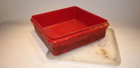
Put the board copper side up in the plastic container filled with etching solution. Use a soft plastic brush to gently wipe the board. You will notice the copper begin to dissolve. It takes about 3-4 minutes to get all the exposed copper dissolved. You just have to watch to make sure it is gone in all areas between the traces. Do not leave the board in the etching mix for too long as the traces will dissolve under the toner that is protecting them.
Wearing rubber gloves, take the board out of t
he etching solution and inspect it to see if all the exposed copper is dissolved. If it’s not, put the board back in and use the plastic brush to brush over this area. If it is dissolved, rinse the board under water for one minute washing it clean. Dry the board with a paper towel.
At this point, the solution is used-up because of all the copper that has been dissolved within it. Dispose of the solution by diluting it in a 5-gallon pail of water. When mixed with the 5-gallon pail of water, the acid level and copper content was well below test limits in the water sample we sent out to be analyzed (restrictions in your area may differ). You may further reduce the amount of copper in the solution by not etching areas of the board that are not required. Consider adding ground planes in large open areas, and using less etchant when making smaller boards.
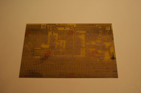
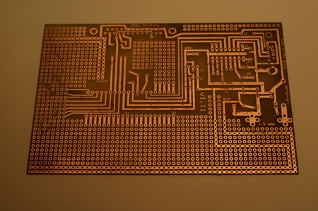
Use lacquer thinner (paint thinner and acetone do not work well) and a paper towel to remove any toner left on top of the copper traces.
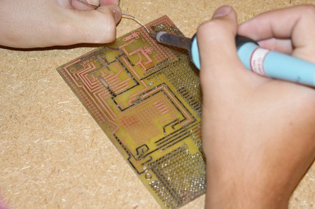
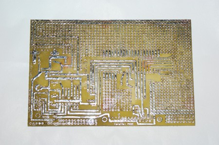
Tinning prevents the copper from oxidizing, which can make it hard to solder to in the future. If you choose, you can tin all the traces with solder and a soldering iron now. This actually makes drilling much easier because it helps to center the drill bit. Make sure to clean off excess flux if you do this. You could use Tinit to chemically plate the copper. Here is a different tutorial describing its use.
Drill all the holes for the through-hole parts using the correct size PCB drill bit and rotary tool. Drill large mounting holes with a normal drill. PCB drill bits are carbide and made to drill through fiber glass that would quickly dull standard bits. There are a few very common sizes of bits and these are often sold in packs. We use .0260″ for IC holes and .0310″ for resistors and caps.
Print out the top side silkscreen layer on magazine paper and iron this onto the top side, using the same processes as above. Again, run under water and peel off the paper. Now you have the component ID’s on the top side.
Here is a different video using essentially the same method:
You can make really nice PCBs of your own circuit design using this simple method, and we look forward to seeing your future projects using this method coming in on the tip line. Look for more How-Tos like this one in the How-To category.





Having done literally hundreds of prototype PCB’s by hand I have to agree with Adam Schabtach and will stick to ferric chloride thanks very much.
I also differ on using steel wool to pre-clean laminate, having used it for decades with no problems whatsoever.
Re: comments about tinning and corrosion. Roller tinning is very nice, but hand tinning with a soldering iron can cause thin tracks to delaminate and lift off the board. If required boards can also be protected with sundry coatings such as varnish, but I have unprotected boards that are decades old and are still in perfect condition (and only ten miles from the sea). A more likely cause of post etching is failing to properly wash the board after etching. The faster you etch the more likely you will get side-etching under the resist.
@norm: “reasons to use home etching;
1 – not everyone lives in the USA and even if they did, no one should settle for postponing a project development for days waiting for a prototype
2 – speaking of a prototype.. it is a “prototype” why pay money for a design that has a high risk of malfunctioning? testing circuit parts, as opposed to software solutions, are relatively easy.. you should build dirt cheap and quick solutions like this and exhaust every possible operating scheme for faults.. then, and only then, you can safely say you are spending money wisely..”
With practice, you won’t be making any more malfunctioning prototypes. I typically design the board, *then* order the board and the parts at the same time.
Yes – you read that right. I design the board and all of the component footprints from the datasheets without any physical parts on hand. I do wait 4 weeks to get the board back from BatchPCB, but I’ve been doing this long enough to know that what I put together is going to work the first time out. If anything, it takes longer to write the firmware than it takes for the board to come back from the fab house.
One thing that helps a great deal is LTSpice. I simulate a lot of my analog designs rather than build actual prototypes so that I can see how the circuit is going to behave before I commit to buying anything.
I’ve been using Reynolds’ Non-Stick Aluminum Foil q
with excellent results.
Don’t try running it thru your printer by itself! Get some laser-labels first, you’ll need them. Preferrrably clear.
1) Print the design on a plain sheet of paper (for alignment)
2) Cut a piece of aluminum foil that’s bigger than your design by at least 1/4″ with scissors (not the cutting edge on the box), being careful not to crinkle it. Make sure to clean up the edges and smooth out any light crinkles, because you don’t want to scratch your printer’s drum or get a paper jam with this stuff.
3) Align the foil, dull side up, over the design printed earlier. Using the laser labels, stick down the leading (top) two corners and as much of the leading edge as neded to keep it smooth to the paper. Keep in mind that the printer will not print in the exact same place twice, and that it seems to help to give the printer at least 1/2″ of empty foil at the leading edge.
4) Print on the paper with the foil on it. It helps to use the print path with the least twists and turns, such as the manual paper tray. If your printer has a cardstock loading tray (on the back, usually) that’s the best.
5) Carefully cut the foil off, trying not to bend the foil much. Cutting the paper might make it work better. The toner is not stuck to the foil very well at all, so be careful nit to jostle it.
6) I use a heat-laminator and run the foil stuck toner-side-down on my copper thru 3-4 times. You should see your design “embossed” in the foil. I assume it’ll be similar with an iron. YMMV
7) Let the board cool, the peel the aluminum off the board. Try to “curl” the foil away from the board, that seems the help.
Etching us the same.
I hope this works for everyone else! I’ve been able to get flawless transfers when I get my board prepared properly. (I have to use dish soap to clean it after using the scotch pad.) It’s way better than scraping injet paper off!
Hey! Nice job here! I’ll be dropping by from time to time :)
HI I THINK I HAVE COME UP WITH A NEW WAY TO ETCH PC BOARDS. AFTER MY FIRST TIME TRYING TO MAKE THEM WITH LITTLE SUCCESS. SO I TRYED AFEW THINGS UNTIL I TRYED THIS .
(1) I USED A SIGN MAKING PROGRAM TO MAKE A PC LAYOUT. THEN CUT IT TO VINYL . WEEDED IT AND PUT THE LAYOUT OVER THE COPPER .NOTE: VINYL CUTTERS CAN CUT VERY FINE LINES .
(2) I THEN PAINTED THE LINES USING A SMALL BRUSH.THE PAINT I USED WAS A SIGN AND AUTO AIR BRUSH PAINT .COMES IN 2 OZ. BOTTLES, THE BRAND NAME WAS CREATEX . I THINK A SPRAY PAINT SUCH AS CRYLON WOULD ALSO WORK, ALTHOUGH I HAVE NOT TRYED IT .I LET THE PAINT DRY FOR A FEW MINUITES. THEN REMOVED THE VINYL .
(3) PUT IT IN ETCHING FLUID AND WOW !! TO SAY THE LEAST IT LOOK GREAT . I ALSO PUT THE ETCHING CONTAINER ON THE DRYER FOR HEAT AND AGATION . WORKED GREAT FOR ME .
I made some PCBs several years ago using a vinyl sign cutter. I just used the vinyl itself as etch resist.
If this link doesn’t work, click on my name.
http://tech.groups.yahoo.com/group/Homebrew_PCBs/files/Sign_Cutter_to_make_PCBs/
Please do not use the muriatic-acid based etchant presented in this tutorial. It cannot be safely stored in a household environment.
Use an safe solution: Ferric chloride or Ammonium Persulfate. Less than $10 at Frys, and other electronics stores.
HI SIR,
Actually m a final year engg student for my project i made own pcb like ur article, my guide teached me well…
My doudt is aft done pcb boards we ve to paint t on the track. which paint v can use.. can u tell me clearly pls?
HI SATZ THE PAINT I USED WAS CREATEX AUTO AIR . THE COLOR THAT WORKED, BEST WAS THE BLACK .YOU CAN FIND IT ON LINE JUST SEARCH THE CREATEX NAME . IT WORKED VERY WELL FOR ME , DAVE
I am trying new papers. If there is a Kelly Paper in your area you can try the one I used last night.
Brand: Wausau
Model: 97101
Label says it is “Exact coated”
This is a nice thin, but better than magazine stock paper with a similar feeling. It is pretty easy to scratch toner off the paper too. I got this for $15 / 500 sheets. Another choice is:
Wausau, 97225
it is “Gloss Coated” and says it is for laser printers. It is a bit heavier than the other paper above and has similar scratching off toner characteristics. It scratches better on my HP 5 laser here at work.
Happy PCB-making!
I have ONE Question. I’ve designed my layout and whatnot. Its all to scale but here is my beef…
To save paper I decided to use B6 sized paper (usually cut it to size by hand) Poster paper works excellent(back side). The paper is aligned in the middle of the paper tray with the stops and so on. BUT whenever I print it. The pdf/ps document viewer prints the image way off to one side and off the paper instead of aligning it in the center. How Do I fix this?
It is so good and understandable i really like it.
There is no need to use hydrochloric acid.
For slow etching use a solution of mono-sodium glutamate (ie food seasoning from the supermarket) and air bubbled through using a fish tank pump.
For fast etching use add hydrogen peroxide solution to the monosodium glutamate solution (ie colour safe clothing bleach, don’t use toilet bleach which is sodium hypochloride).
Ummmmmmmm… I disagree with the comment about not being able to safely store Muriatic acid… I’ve got 4 gallons safely stored right now. Two of the four gallons have been in storage for over 4 years… What, about Muriatic acid, do you think is unsafe for storage in a “household environment”? (bearing in mind that I have two very curious cats, and perhaps I just have a basement chemistry cabinet that locks better than yours does :-))
why not predrill? i do this on almost all my pcbs easier to drill as a hole then etch
i did pcb training workshop. now i need to submit report on it. but i dont know how to begin with this. is there any website from where i can download training report on pcb. please help me…
I am not interested in ciquit board etching. Is there any reason why a regular photo instead of a photo of a cirquit board would’nt work, using this process?
Also, I do not have a laser printer. Using your other option, what is the difference between an inkjet copy, versus a photo copy?
Thanks, Jeff
Yes, you could use a regular photo.
You cannot use an inkjet printer for this process. It relies on the fact that laser printer or photocopier toner is a plastic that is remelted to stick it to the copper surface, where it prevents the acid from removing copper where ever it is.
I set up a Yahoogroup several years ago where you can share questions and information about etching copper, for PCBs or art use. Several artists who acid etch metals have joined.
http://groups.yahoo.com/group/Homebrew_PCBs
tinning a board with high-tin and any less than 3% lead content is prone to the “tin-whisker” phenomenon. see NASA-Goddard
http://nepp.nasa.gov/WHISKER/
“Avoid the use of PURE TIN plated components if possible.”
[quote=Solenoidclock]
July 29, 2008 at 2:34 am
“Ranger, wouldn’t that whisker? Like, catastrophically?”[/quote]
This contributor was likely quite correct (jury’s out on the pun though).
Also avoid galvanized enclosures to alleviate Zinc-whiskers. Cadmium, Gold & Silver do ‘whisker’ too, as do some other metals.
PS: Lead-free Solder should have at a minimum 3% Lead to avoid the tin-whisker phenomenon. Check that NASA site to confirm, especially Toyota Camry owners! (Call it low-Lead. In the long-run better for enviro than Lead-free as less electronics will fail unexpectedly needing diversion from landfills).
If you want to build something that will last in terms of years not months, then ignore these aforementioned effects at the potential peril of your project (future projectile).
very nice method is it Eco friendly .
thank
Mahender Singh
I wonder why the need to drill away so many holes if it is not to reduce the PCB weight..?
Ok, i need something to take high current but not using thick wires like 12AWG or even 10. I have got a copper sheet from an art store meant for hammering into drawing shapes. Thickness about 0.15mm.
Am planning to epoxy down to a layer of glass fiber sheet or kevlar. then do the transfer.. wondering if this thick copper will erode away under chemical well before the toner can take it?
To help eliminate paper jamming in the laser printers, the magazine page used to print on must be equal in thickness to the standard printable paper. I have measured the regular 8 x 11 paper and its thickness is 4 mills ( .004 in) . Several magazines I measured were consistent to a thickness of 2 mills. By gluing two of the pages together the required thickness can be achieved. I used super glue which works well and dries fast. Start by aligning the two pages together on a flat surface. Hold the paper firm and lift the top edge of one paper. Lightly add glue along the edge and let dry. Continue gluing the remaining edges.
Very informative. What program did you use to draw the schematic you printed out?
Also, do you think you could get better results with something other than an iron? A Steinel heat gun, perhaps?
Thanks!!
Hi Guys Please tell me a easy circuit designer software that has an option to export the pcb layout as jpg or gif etc……….
nice…
express pcb proteus & eagle is best software for designing circuit
I know this was written a while ago, but I wanted to let you know the information is still great. I teach middle school engineering and we used this method to teach PCB etching to the students. The iron-on transfer method eventually worked fine for us after a few tries! Thanks so much for the thorough write-up. https://codinginmathclass.wordpress.com/2017/01/09/etching-your-own-pcbs-in-a-classroom/