![]()
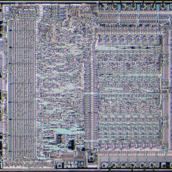
[John McMaster] is doing some pretty amazing work with figuring out how the circuitry in an integrated circuit works. Right now he’s reverse engineering a serial EEPROM chip one section at a time. This is a 24c02 made by ST, and he chose this particular portion of the die to examine because it looked like there were some analog components involved.
He removed the top metal using hydrofluoric acid in order to take this image. By continually removing layers this way he manages to work out the traces and even the components themselves. To help clarify the parts he uses the set of snapshots to generate a colored map using Inkscape. From there he begins labeling what he thinks the components might be, and like a puzzle the pieces start falling into place one by one. From the Inkscape drawing he lays out a schematic, then rearranges the components to make the design easier to understand. Apparently this is a Schmidt trigger.
[Thanks George]


http://en.wikipedia.org/wiki/Schmitt_trigger
I was gonna type “isn’t it Schmitt trigger” but apparently either is okay? Thanks google
hydrofluoric acid??? That stuff is EXTREMELY dangerous, just so you know.
“Hydrogen fluoride gas is a severe poison that may immediately and permanently damage lungs and the corneas of the eyes. Aqueous hydrofluoric acid is a contact-poison with the potential for deep, initially painless burns and ensuing tissue death. By interfering with body calcium metabolism, the concentrated acid may also cause systemic toxicity and eventual cardiac arrest and fatality, after contact with as little as 160 cm2 (25 square inches) of skin.”
Beware.
Watch ‘Breaking Bad’ to get an idea how bad this stuff can be.
Well the main thing about HF is its calcium attacking properties, which make it much more poisonous. Nitric acid would work just as well and be less dangerous.
This is one thing that made me angry while watching Breaking Bad, you would NOT handle hydrofluoric acid in this way. They would have instantly poisoned themselves.
The GDR was specialised in that kind of reverse engineering. Beeing a student in Electrical Engineering in the former GDR, I had the pleasure to see some of the tools they used. Etching, grinding, microscopy.
This was done in Hungary as well. Due to the CoCom list the eastern block could not import high tech. See: http://en.wikipedia.org/wiki/CoCom
So they were smuggled and engineers tried to reverse engineer and manufacture them.
Hydrofluoric acid is not *that* dangerous, if you know what you’re doing, don’t touch it, and don’t spill it on your clothing. (The first aid, if you happen to touch it, is topically applied calcium gluconate, which immobilizes the fluoride ions as calcium fluoride. I suppose any available calcium salt will do the job at least somewhat.) The amount needed to handle etching of chips measures in milliliters anyway. It can still make nasty burns, though; you won’t feel anything at the moment of contact, it will just do bad blisters later as it kills the cells underneath epidermis.
I wonder if the acid could be immobilized in a gel, so it’d be less likely to misbehave and have more tendency to stay put where it is. I did some glass etching in a similar way, soaking the acid into a piece of cotton wool.
Could the chip decapsulation and layer etching be automated? A microscope with a digital camera and motorized sample stage could be used for taking highres imagery of the chip square by square to be stitched together afterwards, some software could be written to automatically or semiautomatically extract chip features and convert them to schematics or annotate them, and perhaps even the etching steps could be handled by a fairly simple robot, at least if the steps don’t need much human attention. A suitable sample holder able to lock to a robot arm and to the xy stage of the microscope (perhaps a magnet?) would do a good job here. We don’t need absolutely exact positioning (though it’d be nice) as we can align the acquired images of the individual layers in the computer by feature-matching. Completeness of etching steps then can be achieved by alternating the etching and imaging steps where the imaging does just a few shots at several places of the chip to determine if the entire layer we want to remove is removed or if another repeat of the etching step is necessary.
We do indeed use Whink for delayering and are quite careful with it. A fume hood, lab coat, and Norfoil gloves do wonders to reduce the risks ;)
While we do all of the decapsulation by hand, John does have a motorized stage for taking images automatically. Some of our data acquisition is discussed in http://uvicrec.blogspot.com/2012/02/tile-stitch.html and http://uvicrec.blogspot.com/2011/12/cnc-microscope-mk2.html. My microscope is fully manual so I leave all of the mass imaging to him.
Impressive microscope setup!
Now the question is if it could be simplified and made hackerspace-friendly (e.g. based on 3d-printable parts).
Actually, you might be surprised at how common HF really is. I used “Whink” rust remover from Wal-Mart to de-layer the Dir**TV HU card and map out the crypto engine back in 2000. Whink rust remover is 5% HF and can be purchased at most grocery stores. It actually works better than 48% HF from a lab due to it\’s staining properties of P-Type silicon, and it takes 5 min or so, as opposed to 2 seconds with 48%. That is too hard to time for individual layers. However, a heated mixture of Acetic Acid and Ammonium Flouride works much better than all of the above for individual layers, because it will not attack the aluminum lines on deeper layers. Even better, try plasma dry etching using CF4 gas. That is best. FYI, Nitric acid won\’t do a damn thing to the glass layers on the chip. HNO3 (Nitric) is only useful to decapsulate the plastic/epoxy case, and only if it has a high concentration of N02 dissolved (aka Red Fuming).. That my friend is more dangerous than a little low concentration HF from Wally World…
I suspect that on the June 10 experiment with concentrated sulfuric that the plastic might be passivating. Try it with a slightly more dilute solution. There might be no need to add another acid
Do as you aughta, add acid to wata.
Mostly I’m curious to leave the gold intact, no sense in making aqua Regia and dissolving the gold before you want to.
I think I heard at last years CCC that someone was working on a program to automate this?
Check out the Silicon Zoo and its gallery of secret things found on microchips.
http://micro.magnet.fsu.edu/creatures/index.html
Perhaps [John] should head over to Visual 6502, where they’ve decapsulated and photographed every plane on a 6502 (and other chips), and then written a gate-level emulator for it: http://visual6502.org/
Might help teach silicon-reading. Also, might want to talk to [segher] of fail0verflow fame, as he reverse-engineered the instruction set(!) of the 4-bit microcontroller used as the security IC in NES and SNES consoles.
We’re already following the v6502 project. Check out our gallery of related work at http://siliconpr0n.org/wiki/doku.php?id=related_work