[Andrew Zonenberg] has crossed a line in his electronic hobby projects. The Ball Grid Array (BGA) is a type of chip footprint which most hobbyists leave to the professionals. But he’s learned the skills necessary to use them in his projects. Recently he ran a test batch to show off his soldering process and illustrate one of the errors a novice might make.
For those that are unfamiliar, the BGA footprint is notoriously difficult to accurately solder because it consists of a large grid of tiny points covering the bottom of the chip. There’s no way to get in there with an iron, so soldering depends on accurate placement of solder paste and chip, as well as a near-perfect reflow cycle. Often times it’s difficult for the professionals too. Many blame the heat-failure of Xbox 360 on the complications of the BGA connects for one of the console’s chips.
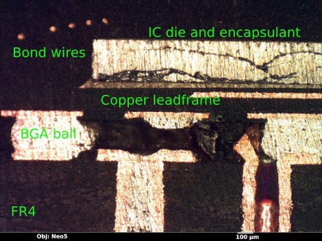
For this experiment [Andrew] wanted to show what happens if you include vias in the BGA footprint. It’s fine to do so, as long as they’re capped. But if a standard via is included, capillary action ends up pulling the solder down into the via instead of making a connection with the chip. The image above is a cross-section of one such uncapped via, seen on the far right.
[Thanks George]


Actually the uncapped via is the middle one. The solder ball has completely wicked down into the via leaving an open circuit. The far right one had a (partialy successful) solder mask dam.
Yep. The original board had about a dozen different configurations of tenting and pad-to-via clearance. Some failed horribly, some worked well, and some were in between (like the one on the right).
The original intention of the board was to see if I could order a board on a cheap process that didn’t support ViP, then figure out some way of plating the holes shut in my own lab using conductive epoxy etc. This was the “control” run I did without any filling so I could have something to compare against.
Actually there’s a ‘simple’ as in safer way I prefer to use, by making my own BGA Socket like for Intels CPU’s. Infact the first BGA I used with a modified LGA 775 socket. Making the sockets yourself though is also not easy, you got to have a nice metal press to stamp out all those fiddly bent pins and patiently solder them onto the board were they wont move. For the socket I mostly just use a piece of plastic with the chips volume milled out. Then the chip clamped down along atleast 2 edges with screws and nuts through the pcb board, if the number of lanes from the chip allows it.
Cool. I’d like to see an article/web page on how you did this (hey, you have my vote for article worthy material). Never touched BGAs because I didn’t believe I could handle the soldering, but a custom socket may be more manageable, to say the least.
I think I covered the process pretty well in the linked article: http://siliconexposed.blogspot.com/2012/07/bga-process-notes.html. Feel free to comment there if you want any more details.
The safe bet is to put the vias all to the side of the BGA pads, the annoying problem with this is that you first put all the vias at the same location in relation to the pad… so the solder paste walks over to the via and pulls your chip to the side with surface tension RUINING EVERYTHING. You have to go back and make new boards with more random via locations. UGH.
Isn’t this what tenting vias is for? Altium->right-click via->”Force complete tenting on top/bottom” or equivalent in Cadence/Mentor/etc. This essentially plates it “shut” I think, preventing solder from wicking down and giving you a very nice flat surface for your BGA.
You can add teardrops to combat the problem Jesse described as well, I think. No issues with a F1152 Stratix II so far following these methods.
Ah thanks, I’ll look into that if I can get over my PTSD on the matter.
Tented vias are vias that have the soldermask over them. In order to get a via under a pad, a via-in-pad (VIP) is used. VIPs are regular vias or laser-drilled vias that have another material filling the hole, often a conductive epoxy that is then plated over with copper. This is how 700-something ball 0.4mil-pitched BGAs are laid out.
Via in pad increases board cost (at least from the vendors I’ve used); standard dog-leg style breakout has worked fine from things like Stratix IIs to BGA Intel CPUs/PCHs. Don’t remember their pitch off-hand though.
It’s definitely nice to afford it, but I don’t think it’s entirely necessary for successful BGA breakout.
I’ve done plenty of successful BGA boards using tented dog-leg vias. Here’s one: http://imgur.com/a/55vkt#0
It’s a single-board computer based on a Spartan-6 FPGA with 64MB of DDR RAM, 128MB of NAND flash, and 10/100 Ethernet.
The FPGA is the XC6SLX16 (I’m making another unit soon with the larger XC6LX25) in FTG256 package – 16×16 array at 1mm pitch.
Does anyone else see an AT-AT?
IIRC the XBOX 360 red ring of death ‘heat’ failure was caused by Lead-free solder! Unleaded solder is not a direct replacement for lead solder; it requires different timing, temperatures, heating and cooling ramps, etc. The XBOX was manufactured with re-flow ovens were set for lead solder, while they used lead-free solder. If the ovens had been configured for lead-free solder, or if they had used lead solder the XBOX RROD failures wouldn’t have occurred.
This resulted in poor solder joints connecting the chips. When the GPU was used it would heat up and cause the board to expand stressing the solder joints. After many cycles of this the poor solder joints would break and the GPU chip now had broken connections.
TL;DR lead-free solder, not BGA technology was the culprit!
Your manufacturer can do everything right and you can still get “RRoD” type problems with lead free solder (mostly on BGAs, but QFNs and other leadless packagess will be ofected by this). Lead-free solder has two disadvantages (not mentioning complicating soldering process.
First, it’s more brittle. That’s why repeated thermal stress from will can crack a joint – even properly made. XBox having inadequate cooling had those cycles pretty deep, and BGA package didn’t help either – on QFP you have legs to soak up some stress.
Second is high tin content. Tin has this nasty ability to form whiskers, shorting your circuits. That’s why NASA gets all their components with leaded solder on leads.