It’s generally pretty easy to spot a microcontroller on a PCB. There are clues aplenty: the more-or-less central location, the nearby crystal oscillator, the maze of supporting passives, and perhaps even an obvious flash chip lurking about. The dead giveaway, though, is all those traces leading to the chip, betraying its primacy in the circuit. As all roads lead to Rome, so it often is with microcontrollers.
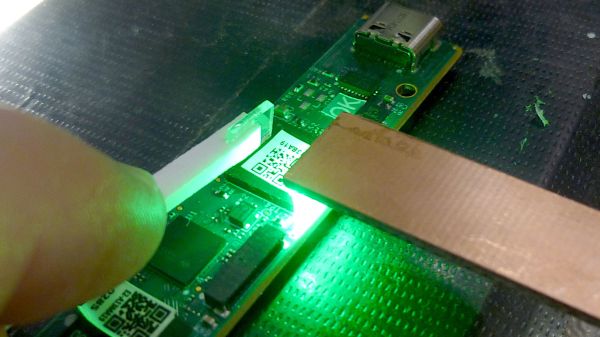
It looks like that may be about to change, though, based on Texas Instruments’ recent announcement of a line of incredibly small Arm-based microcontrollers. The video below shows off just how small the MSPM0 line can be, ranging from a relatively gigantic TSSOP-20 case down to an eight-pin BGA package that measures only 1.6 mm by 0.86 mm. That’s essentially the size of an 0603 SMD resistor, a tiny footprint for a 24-MHz Cortex M0+ MCU with 16-kB of flash, 1-kB of SRAM, and a 12-bit ADC. The larger packages obviously have more GPIO brought out to pins, but even the eight-pin versions support six IO lines.
Of course, it’s hard not to write about a specific product without sounding like you’re shilling for the company, but being first to market with an MCU in this size range is certainly newsworthy. We’re sure other manufacturers will follow suit soon enough, but for now, we want to know how you would go about using a microcontroller the size of a resistor. The promo video hints at TI’s target market for these or compact wearables by showing them used in earbuds, but we suspect the Hackaday community will come up with all sorts of creative and fun ways to put these to use — shoutout to [mitxela], whose habit of building impossibly small electronic jewelry might be a good use case for something like this.
There may even be some nefarious use cases for a microcontroller this small. We were skeptical of the story about “spy chips” on PC motherboards, but a microcontroller that can pass for an SMD resistor might change that equation a bit. There’s also the concept of “Oreo construction” that these chips might make a lot easier. A board with a microcontroller embedded within it could be a real security risk, but on the other hand, it could make for some very interesting applications.
What’s your take on this? Can you think of applications where something this small is enabling? Or are microcontrollers that are likely to join the dust motes at the back of your bench after a poorly timed sneeze a bridge too far? Sound off in the comments below.
Continue reading “Ask Hackaday: What Would You Do With The World’s Smallest Microcontroller?”