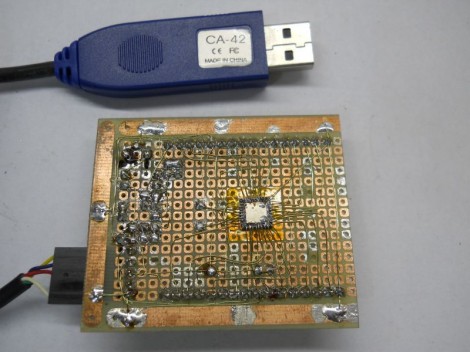
We’re impressed by the ARM prototyping board which [Danjovic] is showing off. He proves that in this day of ever shrinking packages it’s still possible to make your own development tools with protoboard and a soldering iron.
To tell you the truth, if he had designed and etched his own board we probably wouldn’t have featured it. But he didn’t need to spend time on the layout, etching, and reflow. Instead it’s just some enamel wire and a lot of patience. The patience is because the NXP ARM Cortex-M0 chip comes in a HVQFN package. We’re not entirely sure about the HV part (the package alphabet was not entirely clear on this) but QFN means Quad Flat No-Lead. That means no legs on the chip. So [Danjovic] glued it upside down and soldered point-to-point to break out all of the pins.
The top side of the board has a bootloader button, reset button, power regulation, and a crystal oscillator. He doesn’t mention what bootloader he’s using, but a Nokia USB cable gives him the connectivity to push his programs onto the chip.


That is impressive
He is using a stock bootloader that comes with these NXP ARMs, i think, because of the screenshot of the flashmagic programmer that works over UART (rs-232, rs-484, can bus, etc…)
That’s quite a bit of painstaking patience to solder all those lil wires
Nice! though its not to far fetched to get the M0 on a 0.1 inch spaced breadboard friendly pcb. If anyone wants a few for cheap, they’re available for pre-order (femtoduino.com)
How about this:
The Galago is an open hardware ARM board that fits in a breadboard and features the Cortex-M3 version of this chip. It also offers a full debugger on-board and is usable with GCC, GDB and a friendly IDE on Mac, Linux and Windows:
http://www.kickstarter.com/projects/kuy/galago-make-things-better
Sorry for the plug but I designed it primarily for HaD readers like you and I! :-)
Reminds me of Elm-chan’s style. If you’ve never seen it, you should.
Heh, that was the first thing I thought when i saw this.
wow. that’s dedication! most impressive!
well done,should see dev boards become really cheap!
What would it take to build a bot that could automate that ask?
This is very impressive solder work, but I hate to state the obvious: why didn’t he just buy, get a free, development board? They are EVERYWHERE.
I have made so many prototypes from dev boards. Often, the first thing I do is to de-solder all the stuff I don’t need on it other than the uC.
Personally, I’d rather spend my time doing engineering (programming, being creative, putting parts on that are not part of the development board) then soldering hairs to dots. And what happens when the chip fries? Start all over…
Because he lives in Brazil, everything here that is a bit more advanced in electronics has to be imported from USA. And of course, he did it because he can :)
HVQFN – Heatsink Very flat Quad Flatpack No-leads.
Wikipedia’s your friend, after all.
Could be found on the NXP website, too, but not as fast.
I guess editing’s not what it used to be. Like looking up stuff instead of saying “I dunno what’s going on. Look, I’ma scientist”. Bummer.
Which brings me back to the main issue with this article:
This is a nice work of art. I’ve seen more complicated, but it is definitively done well considering the used materials.
But it’s b*s anyways. This is a chip that’ll run at several MHz. The external oscillator even has 14MHz. Connecting it far away by flying wires is like the last thing you want to do when connecting a HF source to a clock input. Seriously.
It’s kind of cool how he manage to solder the ground wires to the heatsink – remember kids, that pad is used to get heat out of the core into the copper of your PCB. Not into the core, out of your soldering iron. Sadly, it works both ways…
14 MHz is by no means HF. Especially not, if the leads are only an inch long.
Soldering onto the middle pad shouldn’t pose a great risk, unless you decide to heat it for several minutes on end. After all, there are thermal barriers in the shape of the Si-die as well as the epoxy attach.
Best regards from someone who used to put silicon in QFNs for a living.
Lars: 14MHz is HF, also known as the 20m band for HAM radio (14.000 MHz – 14.350 MHz) Wikipedia – http://en.wikipedia.org/wiki/Radio_frequency
lol, if 14MHz is high frequency, what are those old pentium 4GHz ICs?
He used .19mm wire.that’s between 32 and 33 awg.They have wire that has insulation that will melt off with a soldering iron. I can do the larger sizes easy. for the smaller you can bend every other pin up to make them easier. It would be great to have a hand tool to make this easier.
This is a QFN. The N stands for no-lead. It basically means no pins. Just flat soldering surfaces.
Bending pins would work on a QFP (quad flat pack).
NXP has M0 in DIP28 now. You can just plug the DIP28 in a breadboard, easiest for prototyping!
The fastest non-BGA ARM in app, and probably the last non-BGA ARM there is, it’s v5, app profile, 128 LQFP
http://www.freescale.com/webapp/sps/site/prod_summary.jsp?code=i.MX233