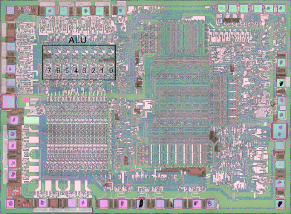
This is a microscopic photograph of an 8085 processor die. [Ken Shirriff] uses the image in his explanation of how the ALU works. It is only capable of five basic operations: ADD, OR, XOR, AND, and SHIFT-RIGHT. [Ken] mentions that the lack of SHIFT-LEFT is made up for by adding the number to itself which has the effect of multiplying a number by two; the same mathematical function performed by a shift operation.
His post details the gate arrangement for each ALU operation. This is clear and easy to follow, and was based on reverse engineering work already done by a team who meticulously decapped and photographed the dies.
Not long ago this explanation would have been voodoo to us. But we worked our way through The Elements of Computing Systems text-book by following the online Nand to Tetris course. It really demystifies the inner working of a chip like the 8085.
Now if you really want to understand this ALU you’ll build it for yourself inside of Minecraft.
[Thanks Ed]


after this semester I too will know and make an ALU for my computer architecture class!
Supposedly the control unit is going to be the hard part in designing my CPU.
It warms my heart that people are still learning such things! Good luck in your class!
Yup. In a purely consumer world filled by cellphones and black boxes programmed in Java, reading the above post made me feel there’s still hope somewhere for students.
Believe me or not but there still are people who think what makes Java to tick and how to make it do faster.
People learning how to program in Java = IT-Majors
People learning how to build ALUs and how to program in C = Electronics Majors
(Disclaimer: I’m writing this as an Electrical Engineering Student)
PS: Admittedly IT-Majors are equally important, because while smart low level programming can improve execution speed by maybe 2-10. Choosing the right algorithm or developing a better algorithm can make a program Millions of times faster.
(Lets compare a Bubble Sort Algorithm written in Assembler to a Quick Sort implemented in Java for a high number of inputs….)
IT-Major here (CE Minor)
I love learning about how things are made from the bottom up. As an unrelated project from my current IT Java class… I implemented a HACK ALU with only NAND gates in Java!
My github project is here: https://github.com/evreichard/jALU
“[Ken] mentions that the lack of SHIFT-LEFT is made up for by adding the number to itself which has the effect of multiplying a number by two; the same mathematical function performed by a shift operation.”
It took me a minute or two to understand this.
I didn’t make sense until I realized it was binary, not decimal.
Then it made sense.
It also works in decimal if you add 10 times.
1 + 1 + 1 + 1 + 1 + 1 + 1 + 1 + 1 + 1 = 10
Although the ALU may seem quite limited, I once disassembled a ROM from an 8085 PCB and found that it was able to run a full-blown RTOS. There is a lot of power in those simple instructions.
There’s a class of architectures called “One instruction set computer” that take this to the extreme. One implementation was featured here recently :
http://hackaday.com/2012/09/05/mess-of-wires-is-actually-a-one-instruction-computer/