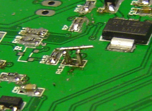
Here’s a collection of tricks to get over some surface mount prototyping issues the next time you find yourself in a bind. But first we have to address the soldering atrocity seen on most of the components above. [Rxdtxd] admits he’s using a firestick for soldering his SMD parts. The non-brand 40W iron is just about the worst thing he could be using (well, we guess a candle would be worse). Try to overlook those joints and enjoy his solutions to a couple of other problems.
First up is what to do when you lift a fine-pitch trace like would be found on a TQFP footprint. The fix for this is to grab a junked transformer and use a bit of the enameled wire from the wrappings as a jumper. The wire is quite fine, and the insulation will burn off when soldered which means you don’t need to strip it first.
The second and third tricks both deal with resistors. As you can see above he placed two 1K resistors on a single resistor footprint to make his 2k resistor. The 0603 packages were both soldered standing on end, then connected with a lead from a through-hole component. The other resistor hack piles five components on top of each other to build resistance in parallel. This is not a great idea as it will fail over the long-term, but it will get you though the prototyping stage as long it doesn’t require precise tolerance.


Why would the parallel resistor method fail over the long term?
It is more likely to lift the pads if shear force is applied to the resistors, it is mechanically unsound so fine for prototyping, not fine for reliability
What shear forces would it experience? A stack of 5 resistors would be maybe 3mm tall and they’re very light. PCB copper is attached pretty well, it’s used to hold mechanical components in place such as surface-mount battery holders and headers. I guess I want Mike’s idea of why it wouldn’t last long; it’s currently an unqualified statement.
Depends on the user. Manhandling PCBs can break any components that stick out. SMD components are fantastic for that reason. However the total surface area of a resistor sitting on end is TINY. It doesn’t take much at all to break that solder joint. A through-hole part on the other hand is more likely to fail at the part rather than at the board, and a properly mounted SMD part is not likely to ever experience any force sideways.
Bottom line, fine hack for something inside a case, not so fine for something that will be used for prototyping.
Additionally, putting resistors in parallel is a common trick for improving tolerance by averaging any difference from the nominal value.
That wouldn’t improve tolerances. The resulting resistance from two 1% resistors put in parallel would still be 1%. No one cares what the distribution looks like, you have to design for worst case.
Additionally, most resistors aren’t normally distributed because of binning.
Has anyone researched the distribution of resistor values? Even if they aren’t normally distributed, they might still have a symmetric distrbution (for example if all the resistors are either -10% or +10%), so averaging them could still improve things.
Film resistors have normal distribution with a hole in the middle. Production process spits out E6 resistors then E12 values are picked out from the middle, from those E24, E48, E96 and finally E192 are picked. [Dave] from EEVBlog did an episode about this.
Resistor distribution is either fairly normal or camel shaped due to binning. [eevblog] did a test of 1% resistors and got a normal looking distribution with no gaps in the middle.
http://www.eevblog.com/2011/11/08/eevblog-215-gaussian-resistors/
The distribution is irrelevant. As engineers (or maker/hacker/artist/student/etc), we must design for the worst case. For a 1% resistor, the worst case is a 1% difference in resistance. For two in parallel, the worst case is *still* a 1% difference in resistance, regardless of their distribution.
If you’re measuring the resistances and tweaking it manually then that’s a totally different ballgame. I don’t think that is what macegr’s original post was discussing, so I wanted to clear things up for people thinking they’d stumbled onto a great tip.
The solder joints would be much more sensitive to thermal stress, but the risk of failure is very very low for a single unit. The largest argument against stacking resistors like this is cost, it has to be done manually and the cost of assembly gets enormous.
Not a problem for prototyping or hobby purposes, but only done in production by chinese…
I once had to do what I thought was a pretty hacky fix. I bought a 2 pin crystal instead of the laid-out 4-pin crystal. We needed to short 2 pins diagonally and then solder the 2-pin crystal across the other pins. Solution? Kynar wire bridge with kapton tape insulating the bridge.
Rules of Surface Mount:
– No Firesticks
– Kapton, Kapton, Kapton
– 30awg silverplated wire-wrap wire will save the day (you can argue over pvc, kynar, enamel, teflon…)
– Don’t be afraid to X-acto
explain the kapton?
Just make a triangle out of them, no need for a jumper.
For fine pitch packages forget about being able to solder individual legs. Just flow a bunch of solder over them, then use solder wick to wick it off. With practice you can do this without leaving any short.
Or use a knife tip to drag all of them at once. Again, with practice you can get all the legs without bridging. Less thermal stress than flooding, I’d imagine.
I love this. It looks like it devolved from a frustrating build (oh, man have I had those) into a comedic tour through increasingly desperate mitigation measures. Especially the parallel resistor tower for a current limiting resistor for an LED. Classic. Any value would have probably worked.
>[Rxdtxd] admits he’s using a firestick for soldering his SMD parts.
I’ve used complete crap irons like this: http://www.maplin.co.uk/30w-soldering-iron-32909 to drag solder big TQFPs and solder wires on to the legs of .5mm pitch parts when doing console mods and it wasn’t really a problem.. The only advantages of having an expensive iron are maybe temp controlled (again, not had much of a problem with fixed irons except for situations involving massive ground planes etc) and being able to get a decent range of tips.
SMD soldering seems to be another on of these things that you guys (hackaday editors) are afraid of … are you guys still having nightmares about building GCC this week?
My community college has an amazing tech ed department for Electronics. The soldering class in particular certifies students for Class 1, 2, & 3 soldering, PTH and SMT, we go from standard PTH resistors to QFN, J-leads, and those super-fine pitch gull-wing leads, in Pb and Pb-free. There were students with physiological issues (hand shakes) and vision problems who could hand solder down to 1206 resistors. Probably would have been better if we had access to proper magnification, all we used were the large lens-on-a-lamp magnifiers that give me a headache. :p
One issue was the flux; we had the worst flux on the planet. On the bright side – I like the smell, reminds me of Grandpa’s office. (Odd considering I don’t recall him doing much in electronics, maybe he just had a piney cologne?)
Instead of putting the two resistors upright, and connecting them with a piece of wire, I just put them at an angle so that the resistors are leaning against each other, and then solder the tops together.
Or even better, since there are no adjacent traces, just form a ‘v’ so both components are flat with one end of each on their respective pad and their tips touching. Upright SMD components are a no-no.
Exactly. That’s also what is recommended in the IPC Quality standard
The funniest part is that the 150 Ohm resistor is used for LED current limiting, and the 2k resistor for transistor base current limit. Both cases are hardly critical, so any reasonably close standard resistor value would have worked fine.
Nice article! When I have to add to resistors in series on a single footprint I usually lean them towards each other, then you dont need the extra wire. You can also make a voltage divider this way if you need one, just solder a wire from the center point. It’s good to see that people dare to do some hobby smd work, it is easy! This article proves that you can do it with any crappy iron.
Soldering a stack of resistors is OK, but in the past I’ve had some trouble with power rating; if you’re already critical this is a no-go; the lower resistors will simply heat up the higher resistors, which also heat up due to their own dissipation, thus putting even more heat in resistors topped on that -> only good if you’re well under the power rating of your resistors.
And please… buy a decent soldering iron, you’re worth it!
I’ve done that in place of a x8 resistor pack that was inverted in layout. I can’t remember the details, but back when I was an apps engineer, a customer came to us asking for help debugging their board. Among many other things (incl. totally screwing up the xtal implementation which was clearly described with pretty pictures and recommended components in the datasheet) they flipped this SMT resistor pack. For some reason I can’t remember I couldn’t just invert the package.
I built it up by hand under the microscope with 0403 resistors and enameled wire over the course of an hour.
Hmm…how about this?;
https://sphotos-b.xx.fbcdn.net/hphotos-ash3/830522_609627269063351_1538510850_o.jpg
R C stacking for sensitive circuits. ; )
Yeah…I know…I’m facebooking my projects….:_(
Nice, it took me a while to figure out the mix of through hole and SMD components, but nice.
Instead of unwinding transformers for magnet wire, get the heat-strippable kind from Digikey, Mouser or whoever. AWG 30 wire-wrap wire is often too thick for fine pitch SMD parts, so we have rolls of various fine gauge magnet wire (a single roll will last a lifetime) in our lab.
And get rid of that unregulated soldering iron! Aside from the poor selection of tips, you’re just asking for lifted traces.
After reading a number of the “firestick” comments, I’d like to ask, is my old Weller WTCP with tips rated for different temperatures okay?
I think they’re mostly talking about no-name RatShack or Harbor Freight sticks. I know every one I ever bought, the tip would oxidize and start to hollow out in a matter of an hour of use-time. It would just burn up. I doubt they had any iron coat at all.
It’s amazing how much difference a decent tip will make. No fighting to keep the tip tinned, just wipe and tin now and then. Even once I learned the ‘correct’ way to clean and maintain a tip, cheap tips will literally dissolve (albeit slowly) in solder.
I’ve been wondering about this, do you have any good tuts on maintaining / cleaning / reshaping tips ?
Why don’t you just instate a one trace per SMD policy?