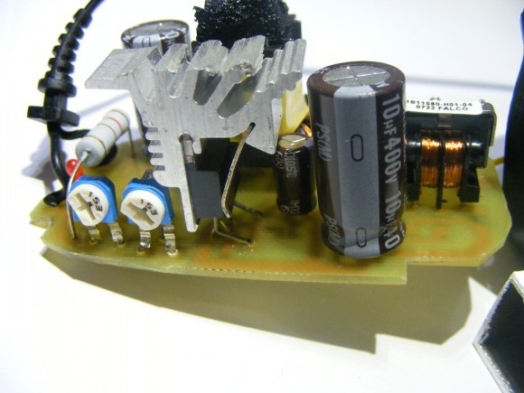
This custom circuit board picks up some of the pieces from a wall wart to drive a high-power LED. The basic concept is to keep the high-voltage components and swap out the low voltage ones for parts that will be able to drive the 10W load.
The PCB is custom designed, but you can see that it was shaped to match the wall wort’s original board. To the right is the original 500mA transformer. The low-voltage side uses an LM393 because of its dual-comparators. This provides feedback for both current and voltage and is a perfect compliment for the TOP242. We haven’t seen that part before, but [Mincior] says that it’s nice for this application as it has safety features that lock down the chip if power or temperature are above spec. Once the replacement is nestled inside of the plastic case it looks stock and makes sure that your custom LED fixtures will stand the test of time safely.


“To the right is the original 500mA transformer” – actually, that’s the common-mode input choke for the mains supply. The switchmode transformer is hiding behind the bit of heatsink.
Hello. I’m the owner of this article. Indeed, that’s the input choke. I’ve just posted the old 500mA original transformer picture to the blog: http://en.electroni-city.com/top242-power-source-for-10w-led/
Without opening the real PCB layout file to verify, I think there’s potentially some fairly serious safety issues with that PCB layout, so I wouldn’t advise anyone copying that design straight off.
Specifically, the creepage distance between the high voltage side and the low voltage side is pretty small around the opto-isolator U2 (I estimate around only a few mm?).
I would have at least 5mm for it to be safety compliant. You will find some standards even call for 8mm or more.
It also looks pretty iffy around RV2 on the same point.
It’s obviously functionally isolated for the most part but you need to pay attention to safety isolation when mains electricity is concerned. That’s what the opto isolator is for, and the reason its an odd rectangular shape (so you can meet minimum creepage/clearances). You shouldn’t be ploughing a track straight underneath the opto – this area should be completely clear (preferrably a slot cut into the PCB too).
Redesigned. Ok. Thanks.
it still seems like it could be better. on the LV side, don’t route the trace under the optocoupler. two minor adjustments and you’ve got a bit more clearance.
on the HV side, it’s a little more difficult and I don’t see a quick and easy way to avoid routing under the optocoupler. However, you can significantly shorten the trace length under it by rotating C8 and C9 180 degrees, moving the big trace left, and running the small trace under D6. I would use a circular corner for the corners of the trace under the optocoupler on the HV side (sharp corners are more likely to arc).
the next thing I’d suggest is trying to find an alternate route for the big trace on the bottom of D7, but I don’t see anything very easy for that one.
Since this is hard to explain, I did a super crappy rough sketch on imgur: http://imgur.com/XerfBJF
I “rotated” those two caps, that’s why the traces swapped sides.
Fixed. I reversed D8 to rectify negative voltage (the other transformer pin) and used TH version of optocoupler. There is enogh room under the transformer to put the optocoupler. Thanks for your sugestion for LV part, did exactly.
I had some of the same initial concerns Dave did but I definitely give props to someone willing to dive into PSU design. Well done. I suspect your original PCB layout is ok since you’re only making one or a few of them and a lot of the rules are designed to deal with variance during manufacturing but it’s great that you were willing and able to take feedback and make the design even better.
When I read the title I read “Wal-Mart” , anyone else?
lol everytime I see the article title.
@mincior: Big props for diving into the project and getting it figured out. Also, thanks to Dave. We all learned a little in a constructive manner :) Everyone keep on tinkering!
HUGE heat sink o_O