We’re no strangers to looking at uncapped silicon. This time around it’s not just a show and tell, as one transistor form a ULN2003 chip is reverse engineered.
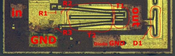
The photo above is just one slice from a picture of the chip after having its plastic housing remove (decapped). It might be a stretch to call this reverse engineering. It’s more of a tutorial on how to take a functional schematic and figure out how each component is placed on a photograph of a chip die. Datasheets usually include these schematics so that engineers know what to expect from the hardware. But knowing what a resistor or transistor looks like on the die is another story altogether.
The problem is that you can’t just look at a two dimensional image like the one above. These semiconducting elements are manufactured in three dimensions. The article illustrates where the N and P type materials are located on the transistor using a high-res photo and a reference diagram.
If you want to photograph your own chip dies there are a few ways to decap them at home.


This should be tagged with silicon not silicone (different things).
Oh, good catch… this tag was an auto-complete error. Fixed.
ohhh my…when i was kid i use to break these in half hopping to figure out the inner workings…as you geussed no luck .but this is way cool
Some large transistors/diodes have very visible PN junctions. The rectifier from a busted microwave had interlaced fingers you could see without magnification. The reflecting sheen is different. The transistors in STKs (TV convergence ICs, motor controllers) are usually bare dies on surfboard inside the casing. Here too you can see a similar interlacing pattern…
Way cool. Good color enhancements in some of the pictures. It should be noted that the diode connection is a common that usually goes to the positive supply, not GND as “painted” into the very nice pics.
Thanks, I’ve added small note about this.
Its nice of you to link to an old HAD Article. Sadly, the link there is already gone.
This article still links to working page :-)
http://hackaday.com/2012/11/21/boiling-acid-used-to-see-chip-die/
Thank you. Very kind.