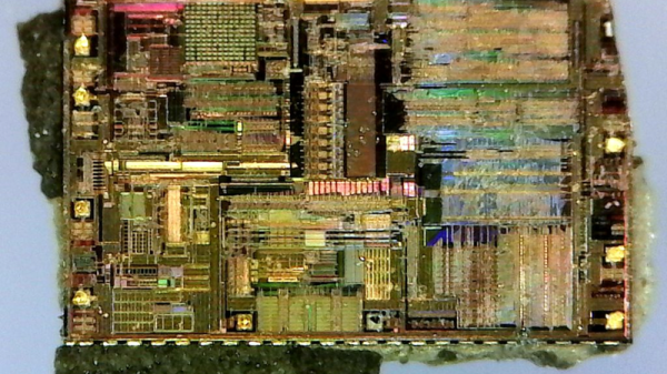
Continuing his reverse-engineering of the Intel 8087, [Ken Shirriff] covers the conditional tests that are implemented in the microcode of this floating point processing unit (FPU). This microcode contains the details on how to perform the many types of specialized instructions, like cos and arctan, all of which decode into many microcode ops. These micro ops are executed by the microcode engine, which [Ken] will cover in more detail in an upcoming article, but which is effectively its own CPU.
Conditional instructions are implemented in hardware, integrating the states of various functional blocks across the die, ranging from the instruction decoder to a register. Here, the evaluation is performed as close as possible to the source of said parameter to save on wiring.
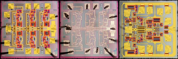
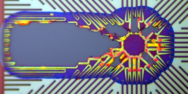
Implementing this circuitry are multiplexers, with an example shown in the top die shot image. Depending on the local conditions, any of four pass transistors is energized, passing through that input. Not shown in the die shot image are the inverters or buffers that are required with the use of pass transistors to amplify the signal, since pass transistors do not provide that feature.
Despite how firmly obsolete the 8087 is today, it still provides an amazing learning opportunity for anyone interested in ASIC design, which is why it’s so great that [Ken] and his fellow reverse-engineering enthusiasts keep plugging away at recovering all this knowledge.

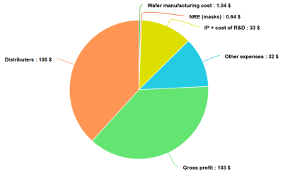 The financial analysis puts Analog Devices’s gross profit at about $103 of the $275 retail purchase price of an AD9361. The biggest slice at $105 goes to the distributor, and surprisingly the R&D and manufacturing costs are not as large as you might expect. How accurate these figures are is anybody’s guess, but they are derived from an R&D figure in the published financial report, so there is some credence to be given to them.