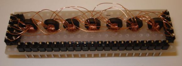
[Kos] tipped us about an article he made presenting his experiences in designing and implementing a core rope memory. This magnetic read-only memory (ROM), contrary to ordinary coincident-current magnetic core memories (used for RAM), uses the ferrite cores as transformers. If you look at the picture above, you’ll count 7 of them. This sets the memory word size (7bits). A new word is added to the memory by passing (or not) a wire through the ferrite holes. If you then pass an alternating current through this wire, a current will be induced (or not) in the other wire turned 30 times around the ferrite (alias transformer secondary).
In [Kos]’s setup, an input pulse of 5V generates output pulses of 15V. For demonstration purposes, he “wrote” a simple program that lights up digits in a seven segment display. Therefore, different numbers will light up depending on which wire he uses to pass the AC current.
These days core memory hacks are few and far between. But looking at this one, and the one we saw in August, makes want more. If you know of any others don’t hesitate to send us a tip.


I wonder if Kos was inspired by the video in the http://hackaday.com/2013/09/10/retrotechtacular-the-apollo-guidance-computer, where the ‘girls’ are handwiring the ROM/?
Most likely. I recently watched that video and always wondered how these worked.
Well, now now it makes a lot of sense.
cool design. but I dont think I would call this memory…
ay! get back to lcd games man!!! 7 bits could be a life/death id and an 8×8 position.
This shit got us to the moon.
This would make an excellent sequencer for a relay-based CPU.
if you know how to make this i dont think youd be using mechanical relays, unless you were making a robot.
Very good article. I was wondering too how these “rope” operates. About relay-based CPU, they are not compatible. Rope memory or core memory generates a very tiny pulse that needs to be amplified (by vacuum tubes or transistors). They are not able to operate relays.
i remember ther was something on magnetic memory where the process was destructive in order to read the memory you had to erase the menory.
That reminds me of the old magnetic bubble memory where magnetic bubbles were propagated across a ferro magnetic material. As the bubble was read at one side of the chip it had to be re-written on the other side so as to re-enter the propagation cycle.
You’re thinking http://en.wikipedia.org/wiki/Core_memory
This is http://en.wikipedia.org/wiki/Core_rope_memory
The only way to erase this is to remove wires.
No: http://en.wikipedia.org/wiki/Bubble_memory
Yes. That applies to the “ordinary coincident-current magnetic core memories (used for RAM)” that they mentioned. The process of reading a bit from core memory (RAM) necessarily zeroes that bit. In order to simulate a nondestructive read, the circuitry had to first read the bit, and then immediately write it back.
http://en.wikipedia.org/wiki/Core_memory#Reading_and_writing
i was told the first moon flight was entirely programmed using a block of these!
Wow that is a Rube-Goldberg way to make read-only memory! I think you can make a bit of memory using a blob of solder– connect to Gnd for a 0, Vcc for 1. Don’t get me wrong, I think it is cool to recreate old and bygone technologies, but in this case, if you are going to all the trouble of hand wrapping coils, make it RAM, not read-only.
If a blob of solder is superior, why did they use this core rope technique on the Apollo guidance computer ?
There’s many nifty uses for a core ROM, because you’re not limited to how many read wires you can pass through.
You can, for example, use 7 cores and 128 wires to produce a keyboard where each individual keyswitch has a wire attached that loops through the cores corresponding to the binary code of that key. Pressing the button down will produce a pulse that generates a corresponding binary code pulse at the output. The pulse will go one way in polarity when the key is pressed, and another way when it’s lifted, allowing you to separate events. Passing DC through the cores won’t produce a pulse, so you can have all the keys down for n-key rollover. (Although the cores may saturate with enough keys down)
To capture the events, you rectify them to DC, and add an eight bit to denote whether the polarity was up or down. This eight bit also serves as a clock pulse to a buffer that catches the signal and stores it for later use.
Lot of people never heard of core memory!
The RAM version was the type invented first. In this, a small core is magnetised by wires wrapped through it in an X-Y grid. North or south. To read it, you have to write it! To read a core, you try and set it to south. If it was north, the field will change and that will induce a pulse in a “sense” wire, If it was already south to start with, nothing happens and there’s no pulse. The sense wire is wired thru the cores just like the X-Y grid wires are.
Obviously reading it in this way destroys the information, since you end up with a south whatever it was. So you need to store your result in an electronic buffer, then re-magnetise the core before you’re finished. That’s core RAM.
Core ROM is similar, an X-Y grid of wires going through cores. Only the sense wires vary. To make a 1, you run the sense wire thru the core as usual. For a 0, the sense wire misses that core out. So a pulse at X-Y will or will not generate a pulse on sense, depending.
Core “rope” is essentially a grid, but for some reason it suited them to knit it in a rope shape. Yep, knit, once they had the design mastered, lots of old women hand-knit megabytes of the stuff, over the years.
It is not only the shape, it is the way that works different. The RAM variand works by setting the core magnetization to right or left. That is, it saturates the core completely. The ROM variant uses transformers in their normal (non-saturated_ operation. That is the main difference (and wiring style of course)
This is superior to a blob of solder, as a blob of solder isn’t addressable, while this one is. Try to make a decimal to 7 segment decoder using only blobs of solder…
That’s what mask-programmable ROMs are, silly.
mask-programmable ROMs needs address decoders and, at least, diodes.
You need diodes to adress the blob of solder.
I remember this !
RAID (USSR clone of IBM Mainframe) or Polish Odra has these kind of memory.
with Regards
Pawel
a similar technique has been used in old jukeboxes:
a theory of operation can be seen in this article http://www.flippers.com/Seeburg-tormat.html
Tormat. What a name! They still work in one I have worked on, just big enough to slip a ferrite on the end of a pencil. Not as tiny as IBM core.
IBM 360/40 (circa 1964) used transformer core as its microprogram ROS. (there are some pictured on the web)
S/360/30 used capacitive ROS; similar idea, but using a card as a bunch of capacitors.
Hello guys,
Yes indeed this is a core rope memory. It is a ROM not a RAM, as magnetic core memory is.
The 7-bit word size was chosen to drive a 7 segment display, there is no other reason.
The word size can be more, by adding more cores. There may be a situation where is lots of cores exist, the last cores cannot be driven so hard, so another design with inhibit wires is needed. But for low number of cores no inhibit wires found to be needed and this simplifies design.
The number of words can be increased by simply passing more wires through the cores.
Note, this is only the “storage” array, there is no address decoder.
Actually this wired like an IBM TROS memory. It has has fixed sense loops and the data is woven in the address lines, whereas rope memory had the data woven in the sense loops.
I think that this is a splendid retro hack. If it was good enough for Apollo, then that’s good enough for me. Imagine your code being hard wired. How good would it have to be ? That’s my definition of ROM. I had the pleasure of working on the GEC 40/80 in the 80’s and we’d lift the lid on the core RAM, take a breath and look upon that grid with great reverence. All core work is devastating in its detail.