One of the benefits of plain text file format is that you can go in and edit them by hand. This is part of the KiCad board outline hack which [Clint] wrote about in a recent post. He wanted a unique board outline, which is something that KiCad isn’t necessarily well suited for. His solution was to create the outline as an image, then import it. If you’re wondering what custom shape is called for this type of work we’d like to point you to the (kind of) bottle opening HaDuino. That PCB layout was done on Eagle, which has a bit more leeway with special shapes.
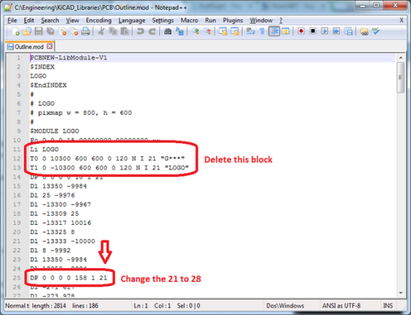
Before getting to the code editing step seen above [Clint] used the built-in feature for KiCad that will turn an image into a component. He exported that code and altered it using a text editor in order to change the layer setting for the shape to that of the board outline. This took him from a plain old image, to a module which can be selected and dropped into the board editing program. It’s a snap to do this sort of thing for the copper layers too if you’re interested in using your mad graphics editing skills to layout an art piece on copper clad.


Well to be snarky, this isn’t so much “in kicad” as “outside of kicad” or “despite kicad.”
Hopefully this feature will be supported for real some day.
you could make a rectangle board and use dremel with router bit and jig to grind off the edges to make the shape you need.
if you just need to fit inside of screw posts you could use tin snips and cut the corners off making an octagon
Thats a pretty retarded way, even more if you are sending the boards to be made professionally..
Can any one point me to a nice kicad tutorial? Thanks.
So far I found best resource page of users tutorials for KiCad: http://www.meatandnetworking.com/w/Kicad_Resources You can search tutorials on YouTube if you want to. Although is good practic to use KiCad developers tutorial, wich you can find in their homepage.
When i started use KiCad, i’ve been curious about drawing not regular board shapes. Well.. Again digged over internet and found this forum source: http://electronics.stackexchange.com/questions/68381/elliptical-board-edges-in-kicad-or-circuitpro Here is similar idea to this article and few another helpful ideas.
P.S. Remember, when you start work with KiCad be patient. KiCad has some tricky parts for absolute beginners, especially when you already worked with EagleCAD. And sorry for my english mistakes. I hope this was helpful.
Thank you.
The problem with this is when making a PCB where the outline is defined by a DXF e-mailed to you by a mechanical engineer who is designing an assembly you will never see.
Or, when you want a specific shape to be dimensionally accurate without the joy of pulling teeth.
Despite that, kicad is the best open source layout tool that I am aware of.
I actually wrote a tool a while ago to convert DXF files to Kicad PCB files. You can find it at http://andygoetz.org/2012-9-13-complex-shapes-in-KiCad.html
Andy, your resulting board outline looks amazing!! Great work!
This is a stupid question, but how do you execute your .cpp file? Should I put this into a new VS 2012 Express project? I was hoping to find you had a batch file, executable, etc… that could be downloaded and run.
Would be nice to have your code as an import DXF option directly in Kicad, could you not submit your code as a patch?
Yay, Kicad!
well, is is actual a lot easier than posted here. I draw my pcb in inkscape and make it one outline using union and difference. then i delete all the not used layers and save it as .plt (HP graphics language format [AutoCAD]) i open the plt file again with inkscape and export it now as a dxf. all curves will be converted to a multitude of straight lines and can be imported straight into kicad with the import option in PCBnew. ver. 2013-12-14
Thank you! Worked perfectly!
You can get inkscape extension scripts from https://github.com/erichVK5/inkscape2pcb which will convert paths into pcb-rnd layouts or gEDA PCB footprints (.fp) which are compatible with Kicad.
The paths are converted into linear elements.
Have fun!