Many of our readers took the habit of using Eagle to design their PCBs. Even if you’ll find plenty of support for this software as well as a lot of parts libraries, the software comes with limitations. The useable board area is limited to 4×3.2 inches, only two signal layers can be used and more importantly the schematics editor can only create one sheet. On the other side, some of you may already know KiCad, a free open source and unrestricted schematics and layout software. [Chris] just tipped us of a video series he made, showing people how to design and build their very first PCB using this software. It’s a simple 555 circuit, but goes through all the steps necessary to design a PCB that costs only $5 through OSHpark… and will blink by the end. All the videos are also embedded after the break.


Thanks, I was searching to do a bigger board than what’s allowed with Eagle, that is exactly what I needed, in the right time, great!
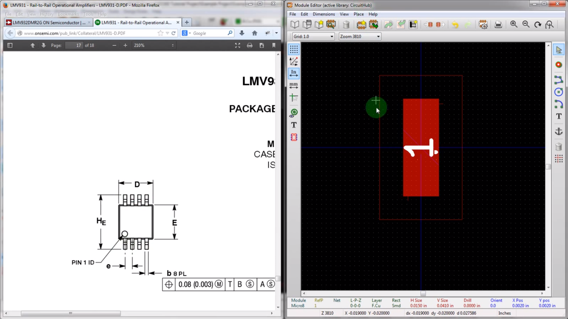
Wrong video is listed for #3 (original site has been updated with the correct video also) – should be http://www.youtube.com/watch?v=SiL9Xdxtw_E
thanks Richard! post updated…
Yay! KiCAD!
Go Hack a Day!
Would be useful to know how KiCad compares with the full blown commercial version of Eagle when using the software to develop products commercially In the event Eagle is superior in that regard it may make sense for the hobbyist live with the limitations of using Eagle for free. One may not remain a hobbyist forever. I could be wrong, but in my mind being somewhat familiar with Eagle could be a plus later in an electronics related career. Then again being familiar with both couldn’t hurt.
As an over-simplification, you won’t find either in a corporate environment. However, that’s not really what you were saying. I’d say full blown EAGLE and KiCad are comparable. Each have quirks, each have benefits. I’ve used both and I prefer KiCad (hence the reason I made these videos).
If you’re looking at trajectories, I think KiCad has brighter days ahead. Yes, EAGLE also has the CadSoft team in Germany working on it, but they are limited by the size of their company. KiCad has the benefit of being an open source project, which means the team COULD get infinitely big (it won’t, and we wouldn’t want it to anyway). But this also means that groups like CERN can jump in and assist with development, causing accelerations in capabilities and features: http://www.ohwr.org/projects/cern-kicad/wiki/WorkPackages That’s what has me most excited.
No doubt Chris is getting rich off of this: Richer than Joe Grand and his security talks! ;p
“But this also means that groups like CERN can jump in and assist with development, causing accelerations in capabilities and features:”
I see what you did there.
“As an over-simplification, you won’t find either in a corporate environment.”
Our company, as well as about a dozen others that I’m personally aware of, use Eagle Pro. I’m sure there are many more. It fits our needs perfectly with 6 engineers and its really easy to pick up and get going. We use schematic capture and layout. We’re not fond of autorouters so we don’t purchase it. We dropped OrCAD 9.2 many years ago and we haven’t regretted it since.
I looked into KiCAD again a few months ago and found it still too rough around the edges for our needs, although some nice progress is being made. I’ll keep watching its progress.
When CERN makes KiCAD have all the capabilities of Altium Designer then I will use it.
Good for you!
Let’s not be lazy and contribute to the project if we can! We cannot depend on CERN alone for everything. KiCAD has a lot of potential that we the community can make a reality!
I think the FPGA design capability of Altium Designer could be ommited ;-)
I am not sure “we” would really want that.
Of course Altium Designer is a very good tool – but – the downside to that is that there are so much functionality in Altium that the casual user, the hobbyist, the student user, will not be able spend enough time with Altium to get really good at using the tool.
KiCad is “good enough” for most things that can be produced by one person and cheap enough to use in hobbyist and school settings.
CERN uses Altium Designer too, but it is much easier to have students/interns use KiCad: There is no license management, no per-bum/per-feature/per-cpu fees to measure and no design repository server for a newbie to screw up. Just download, Install.
I contend that if you need a multi part series to show you how to create a design for a 555 based blinking LED in kiCad, that this is just further evidence of how insanely horrible the interfaces for most electronic design software is, and how steep the learning curve is for somebody who just wants to knock-together-a-blinky.
If being an EE is your job, fine, spend 6 months coming to terms with an arcane interface, but for casual hobbiests, it just shouldn’t be this stupidly, grotesquely, ridiculously unintuitive.
You CAN make an intuitive, easy to use, and capable design package, look at Fritzing (make sure you use the latest current release if you take me literally and try it) for example, ok ok it doesn’t have anywhere near the capability of a “real” electronics design package (it’s not intended to, it’s a teaching package), but what it IS, is for the most part intuitive, you can sit a “noob” down in front of Fritzing and it is CLEAR how to do things. It works in just the way somebody without prior knowledge would EXPECT it to work.
Of course, the biggest market for these software packages is not a hobbyist struggling with a blinky design, but people designing a real board. Bigger projects require more advanced features, and more features have an unavoidable consequence of increasing the learning curve.
The point is that KiCad /is/ an industrial-strength layout package. But hobbyists get to use it too. For free!
Furthermore, if I make something in KiCad I can give it to you, and you don’t need to spend any money to use it. If I made something in Eagle that was bigger than their free limitations allow then it’s useless to you.
For a simple 555-based blinker you wouldn’t need a CAD package, just a sheet of paper and a marker pen for drawing the traces on the PCB you’re going to etch. But a simple project that anyone could do on paper is exactly what you want, from an educational point of view, for a tutorial. Because it allows the student to focus on using the program, without the distraction of trying to understand the project being used in the tutorial.
Bingo! If you want a complicated project with explanations of all the theory and design decisions being made, that’s what I’m doing in Contextual Electronics.
I watched two of the vids and honestly, they could be a LOT shorter. There was a lot of “hmm, it didn’t like that…”, “oops, let’s try that again”, lots of redrawing of lines that took forever etc. Personally I got really annoyed and couldn’t finish.
In another article about KiCad I wrote some links about KiCad tutorials. Check this link: http://hackaday.com/2013/10/15/creating-irregular-board-outlines-in-kicad/#comment-1076447
I think, is better reading an tutorial in PDF, than watch long videos wich are uninformative as You said. Likely not all of them such is.
I agree, the videos should have been shorter. However, if I compare it to Jeremy Blum’s treatment of a very similar circuit (embarrassingly so, I didn’t realize it until after the fact), he takes about the same amount of time to explain things in EAGLE (1.5 hours compared to my 1.75 hours): http://www.youtube.com/watch?v=1AXwjZoyNno&list=SP868B73617C6F6FAD
So, it is what it is. I wanted to try and touch on all of the topics that are necessary to get a design done when you don’t have all footprints and schematic symbols available and I think I achieved that…even if it wasn’t the most linear fashion.
If you are looking for a simpler interface, I think Upverter does the job well (and in a no-hassle fashion since it’s in your browser). I think the back end is limited though on what they’re able to do right now, so I thought I would show the front end of KiCad to try and get people a little further up the learning curve.
I agree. The biggest issue with all EDA programs is to make the footprints. I’m used to mechanical CAD programs like SolidWorks and its ridiculous that it takes an experienced EDA user hours to make ONE footprint, in 2D! I can do the same footprint in 5min in SolidWorks and export it to the EDA program. In 15min I would have modeled up the physical package for the assembly.
CAD stand for Computer _AIDED_ Design and that might be the reason why EDA programs are not called CAD because they don’t really aid you in designing. Like why are there no driven dimensioning tool, only measuring tool? Inserting coordinates for lines and circles in a command prompt, wtf? Its 2013, not 1943. Please take a look at the 2D capabilities of a modern mCAD program.
I agree, all EDA software I tried had horrible CAD capabilities. I was using Eagle for many years and found it a PITA to make footprints, let alone making precise placing of components with mixed mills/mm grids. Recently I moved to Altium 13 for a bigger project that would be overly complicated on Eagle. It took me a couple of days to get fully used to it, but now I love it, and making new footprints it’s a matter of minutes (less than five most times). The project’s structre is very polished. I have a project with 3 pcbs, 15 schematic sheets, and a couple of custom components, and it’s all very well organized.
I have never used Altium but it looks like how a modern EDA software whould be like. But still, is the footprint making any better? One major advantage is the export of IDF 4.0 though.
Yes, making a new footprint is really easy. Just add a new pcb library to your project, and place pads and overlays. Then you can use that with schematic libraries you already got, or make new ones just as easy. The interface for the footprints and pcbs is the same, making it very easy to use. You can place pads with different shapes, specify to which layers they connect, and so on. Much more powerful and easy than Eagle. There are also wizards for making footprints, but i’ve never used them. Just look up “altium footprint” in youtube to see how it’s done.
For anybody still on the fence about whether to use KICAD or Eagle, I say go for KICAD! I think KICAD has not gotten the exposure it should. Like was mentioned above, it is an industrial strength solution, versus the free version of eagle with the pile of restrictions associated with it. Give KICAD a shot! The day KICAD gains all or most of what Altium has to offer is the day Altium probably starts really loosing some business. For all its features, Altium really does have a lot of bloat for somebody who isnt going to be designing FPGA stuff, and truth be told, some of freely available IDE setups for FPGA’s are much better anyway. I have used Altium, KICAD, and EAGLE. While Altium is a lot more polished than KICAD at this point, KICAD is almost there. Eagle is stuck in the DOS ‘TANGO PCB’ days as far as the interface is concerned(ever used old dos ORCAD?), so it has a very long way to go to catch up. As an added bonus, the KICAD file formats are all text based, making recovery, repair, and hacking them (if you needed to) very simple! Try doing that with an Altium file, let alone fixing one that got corrupted!
I agree. I’ve been using Eagle for 13 years, and I’ve suggested ways they could be more helpful to the OSHW community (http://www.xess.com/blog/a-modest-proposal-to-element14/). Their response has been jack-squat. So I’m looking at Kicad for a version of my XuLA FPGA boards. These tutorials are just what I need to get familiar with Kicad. (Hey, why read a tutorial when I can just sit back and listen to the dulcet tones of Chris Gammel for 1.75 hours!)
Good point about the hacking. The python integration that’s in some of the prerelease stuff is really quite exciting. That will open up the program even more to all of the script wizards out there (a group I am not yet part of, sadly)
I have used Orcad. In my experience DOS Orcad was the only good Orcad! The initial windows versions were so buggy that they were useless. Recent Orcads still looks crap’ish and feels dodgy, somehow (IMO).
I have a lot of experience with Eagle and zero with Kicad, so I really tried to watch the videos, I got as far as the 5th one where you spend almost 20min to create a simple 8 pin custom footprint and gave up after cringing alot. I have to wonder, is this a Kicad limitation or is it perhaps a limitation of your skills (not trying to be mean) but the same think in Eagle would have taken less than 5min for a complete definition of the symbol, pads and device. Specifically placing the pads at the correct coordinates, in Eagle I would have just set the grid to the required spacing then I would have just placed the pads one after the other bang, bang, bang, done and they would just snap to the grid at the correct spacing, instead of hunting around for the coordinates like you do in Kicad. Is this really the best Kicad can do?
Instead of watching the video you should have spent the time playing with KiCad. Since you are already experienced in the art you should know what you want to do, and you should be able to figure out how to do it in KiCad. There is no substitute for having a go, and because KiCad is free there is no reason not to.
If you did that you could answer your own questions, and furthermore, your experience might make it more likely that you would use KiCad more efficiently than the guy who made the tutorial.
I have done a few hobby layouts, and I was able to jump straight in with little difficulty. Every time I needed to do something that I couldn’t see was obvious, a quick Google search found me something that got me unstuck.
I tried KiCAD. I gave up after looking at the library. Really, the stuff that it comes with didn’t make sense to me. I couldn’t find anything. Naming your components with one letter, really?
Tell you what. Re-do the entire library to something human readable, then I’ll give it a try.
Oh, and no back-annotation? It’s 2013, not 1943.
Perhaps there was something wrong with your installation?
My install have a button “Library Browser – Browse Library Components” which does indeed do exactly that – with little pictures too. Components have the kind of library names that they usually have in libraries. Components, when placed on drawings use single-letter+digit names, this is a standard and works the normal way. I haven’t tried if one can type more letters in the name field, I think one can.
I managed to do a hierarchical design with KiCAD, I think it could be easier to set up but it does works by following the instructions. There is a bug in the hierarchy viewer – one has to open it on the “top” schematic in the hierarchy or it will not know where the “root” is.
I have used KiCAD for a while now and even used it to make boards that I’ve ordered from iteadstudio. I’ve also used eagle to order from Sparkfun’s service. KiCAD is a little better than eagle I think. It has a learning curve just like eagle but it’s powerful and opensource. If you don’t like to be locked down by software then I’d go for KiCAD. Plus it’s multi-platform.
BTW: I used this series to learn KiCAD. Awful robot voice but good instructions
Doh: http://www.youtube.com/watch?v=rkQ0nVX1q1k