[Quinn Dunki]’s Veronica, a homebrew computer based on the 6502 CPU, is coming along quite nicely. She’s just finished the input board that gives Veronica inputs for a keyboard and two old Nintendo gamepads. [Quinn] is building this computer all by her lonesome, including etching all the PCBs. She’s gotten very, very good at etching her own boards, but this input board did inspire a few facepalming moments.
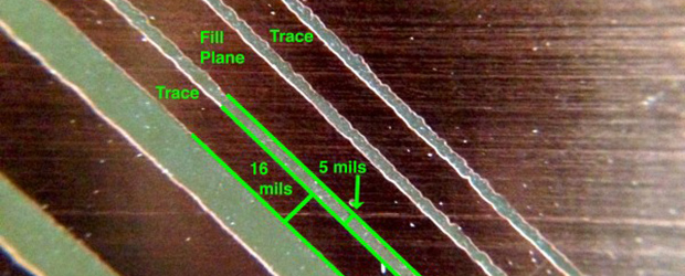
In an earlier post, [Quinn] went over her PCB etching capabilities. As demonstrated by the pic above, she’s able to print 16 mil traces with 5 mil separation. This is just about as good as you can get with homebrew PCBs, but it’s not without its problems.
[Quinn] is using a photographic process for her boards where two copies of a mask is printed on an acetate sheet, doubled up, and laid down on a pre-sensitized copper board. The requirement for two layers of toner was found by experience – with only one layer of toner blocking UV light, [Quinn] got some terrible pitting on her traces and ground planes.
Two photographic masks means the masks must be precisely aligned. This example shows what happens when the acetate sheets are ever so slightly misaligned. With a 5 mil gap between traces, [Quinn] needs to align the masks to within ±2.5 mils; difficult to do by eye, and very hard once you factor in flexing and clamping them down to the copper board.
Even when this process goes perfectly, [Quinn] is pushing the limits of a laser printer. When printing at 600 dpi, the pixels of the print are about 1.5 mils. While GIMP, printer drivers, and the printer itself have some fancy software to help with the interpolation, [Quinn] is still seeing ‘bumps’ on the edges of perfectly aligned parts. This is one of those things that really makes you step back and realize how amazing fabbing PCBs at home actually is.
With most of the hardware for Veronica out of the way, it’s just about time for [Quinn] to start programming her baby. We’re not expecting a full-blown operating system and compiler, but those NES gamepads are probably crying out for some use.


5 mil is seriously good even for pre-sensitised boards. Especially with doubled artworks, Quinn’s hands must be a lot steadier than mine to align those two artworks so precisely.
I use dry film and single tracing paper artwork but I seldom bother with 10 mil separations let alone 5. Better things to do than try and find and fix hairline shorts.
Actually get yourself a good stereo scope for SMD work. you can align it quite easily that way when you have magnification. The hard part is you need to find a light source that you can use that will NOT start exposing the boards. I discovered that the LED light source on my surplus unit was putting out enough UV to actually start exposing boards. I added two panes of standard window glass to solve that issue. (Glass blocks UV significantly) But I need to build a better more board safe light source for the bench anyways.
Change the LED to red spectrum LED. If you pick a white LED, it may have a range of light spectrum that can include UV. However, LEDs unlike incandescent or other light sources can have very specific and fairly narrow spectrum of light. Choosing RED or close to that spectrum is far enough away from the UV spectrum that you shouldn’t have any UV generated from the LED itself. You can also use a red filter. If you have a uv source strong enough to begin any noticeable etching, it is probably strong enough UV to expose photographs. Generally, this stuff should not be quite as UV reacting as the photosensitized coating in traditional photography.
A simple red or orange light would be sufficient. Think about what they use in semiconductor labs. If you can manage that, you should be okay regarding UV exposure. You shouldn’t need to be in a photography darkroom. I would also caution a note of any fluorescent or incandescent light bulb or otherwise in the room. You might just use a detached light source near by and not use the Light source of the microscope.
Red and orange light is far away from the UV (opposite side of the light spectrum) from UV. That’s my suggestion. White light by definition basically composes of red, green and blue spectrum light or it is full-spectrum which would mean that the light generated has a wide frequency spectrum from around 400nm to 840nm. So if the LED is what they basically call full-spectrum (whether visual full-spectrum or the LED types used for growing plants)…. it’s basically going to have a little bit of UV. Most UV sensitive coating isn’t necessarily sensitive only to UV but near UV like violet and even blue that is close. It depends on the frequency range sensitivity of the coating used on the PCB.
While glass helps, you can also choose specific color LEDs for light sources. In addition, you would not want to be working directly to sunlight or light coming through windows. A limited amount of indirect light in a room should not have enough UV to be exposing your PCB prematurely under most circumstances. The UV sensitivity should be comparable to diazo and cyanotype photo-emulsions but I can say they are the same as they are not the same chemistry.
instructions unclear…used low iron glass :D actually a local glass guy was able to get me a sheet of this for wayyyyy cheap, like half of what i could get quotes for online or calling glass suppliers. weather stripping, an ebay vac pump from china and a 3 layer plexi sandwich under it with parts subtracted from middle layer and holes in top… allows for vac pull down. I just happned to get lucky the first time with vac power from 12 buck china pump and thickness of glass, ymmv. had to move and havent diyed a board since…but i have a scope now so im looking forward to how much easier it should be.
These “bumps” on the edges might not have anything to do with the printing, but rather be and artifact of the etching process.
I suspect so. In some of the boards I’ve etched, even though the transparency has a pretty dead-straight edge, I still see little bumps. I wonder if it’s because the copper is maybe a slightly different thickness over the strands of the fiberglass weave in the board material.
Branded toner, although more expensive, is definitely more opaque (at least HP is). I used to be able to expose boards with only a single transparency when I was using HP toner, but now I definitely need two transparencies with cheapo toner.
I don’t know about track spacing, but I was able to etch down to 4mil _wide_ tracks when I did a test ages ago –
http://imajeenyus.com/electronics/20130322_making_pcbs/photos/smd_and_tracks.jpg
Note, the transparency for this was printed on a big office machine capable of at least 1200dpi. No way would I actually trust a 4mil track though! Generally I go for 24mil for simple boards, 16mil if I need to get between pads, and 10mil if I’m really stuck.
I used to have this problem alot when screen printing. Having to use two sheet per print with my laser, to get a dark enough mask for screening. I switched not long after to using velum or semi transparent tracing paper, It holds ink/toner so much better. Not only that but it has a more even tone all over when you hold it up to the light.
The stuff i use is Daler Rowney tracing paper, it’s 90gsm and work well in laser printers ( just remember to set the printing option for velum/tracing paper or plane paper if there isn’t one. For the exposure time it’ll take slightly longer but that’s generally because it’s opake, I always use a glass pane over the paper to make sure that the mask is super flat against the surface to give tighter/sharper lines.
http://www.amazon.co.uk/dp/B004BF4M18/ref=cm_sw_r_tw_dp_AHHYsb0844VJH
That certainly is a problem with immersion etching. Can be avoided using bubble agitation in a vertical tank or better with spray etching that allows finer track spacing.
Surely the pixels at 600 DPI are 600/2.5/1000 = 0.24mil
Eh? One inch is 1000mils. You have 600 dots per inch. Therefore one dot is 1000mils/600=1.6mils.
I think you’ve got confused and thrown in some millimeters there as well ;-)
I was wondering what unit mils are (more metric then imperial in Europe). Weird that the US still loves the imperial measurement system.
http://cdn.zmescience.com/wp-content/uploads/2011/03/metric-system.png
Map over imperial and metric. The red patches are the last countries that uses the imperial system.
Funny but when I watch Top Gear they use miles per hour and miles per gallon as do many UK car maker websites.
Actually Canada also uses the imperial system…. we’re not really 100% metric like Australia or Europe. Weather is metric, but cooking temps for ovens is imperial, we use square feet not square metres for property, people say their weight in pounds not kilos, the hardware store sells wood product in inches, the electrical wiring is american gauge not mm2, pressure is in PSI not kPa… so you see it’s not that metric up here!
To me, mil is short for millimetre, and thou is short for thousandths of an inch.
Same. I do a lot of work in build shops for the auto industry. Depending on where you are in the world, I’ve found “mil” means up to three different things for linear measurement. In thousands of build shops and engineering firms in North America a “mil” is short for millimeter, a “thou” is short for thousandth of an inch. In some very old firms ( from revolutionary times) on the USA east coast, engineering shops term a “mil” as one millionth of an inch. Those are very rare though. Common use in modern machine shops for extreme tolerances is microns and thousandths with 0.001″ being very tight tolerance for common machining and 0.005″ considered normal. Most USA car manufactures want a bumper to bumper tolerance of around 0.004″ Realistically they get around 0.02″ eh /shrug terms :)
With Inkjet, 600 dpi is your ink dot width not necessarily your pixels per inch level. Usually, there is about 2×2 to 4×4 dots per pixels. This usually means you have about 150 to 300 ppi for a 600 dpi inkjet. As for laserjet, is also an ink based technology using a type of ink called toner which uses laser to create a static charge. I would argue they would have about the same PPI level as the inkjet for the same DPI. Reason is, pixels are roughly squares but the dots aren’t exactly square but more spherical so it takes an array of dots to form the square pixels.
Therefore, you’ll be likely pushing your best luck at about 4 mil traces for a 600 dpi print. Therefore, step it up to a 1200 dpi or 2400 dpi printer for better PPI resolution and maybe handle about 2 mils or even 1 mils traces. That is about where you want to be to handle some of the parts working at 0.4mm pitch or you better draft by hand using .13 mm and smaller nib size technical pens.This is where stable drafting, a drafting rule edge would be very helpful. This is where professional technical hand drafting skills will come in handy and is not for the timid.
Nice 4800 x 4800 dpi printer would be good to have or if you plot 24 x 36 mylar, a plotter with this resolution would come in handy.
As long as you’re parts are so darn small, you should be ok.
Bottom line: there is a minimum reliable line width that can be printed at 600 dpi because actual ppi is usually less than the dpi because of the interpolation of dots. You probably want to be using printing resolution up at the 2400 x 2400 dpi level for clean lines in the 1.5 mil size. However, there is always going to be fuzzy edges but it shouldn’t be noticeable to the human eye. It should be fairly sharp.
mils in PCB do not refer to millimeters :P
And anyway, SI notation for millimeter is “mm”.
My bad ignore that…..
Inkjet printers are so much better than lasers for photo exposure. I use a Canon MG5250 set to T-shirt printing mode and get a lovely thick black print that’s perfect for UV exposure without doubling up. I’ve been getting TSSOP happily with my first etching attempts and going to try LQFP soon.
The uneven edge to the traces is probably not due to the exposure but needs tweaks with the etching process. Slow etches can cause this.
Agreed. I always had trouble with the way the fuser of a laser printer distorts the transparency, especially when doing double sided boards. I use an HP Deskjet at it’s highest DPI and turn the black way up and I can make 8 mil traces. Also I don’t need to double up. I also agree slow etch causes problems, that’s why is so important to use warm etchant and agitate constantly, using a foam brush to wipe down that board now and then.
Using GIMP might be the cause of “pixeling” as it raster graphic program. Exporting as PostScript and feeding directly to printer might increase precision. Even if printer is said to be 600dpi normally it can be better than that.
Toner transfer method is easier and once you get the hang of it, more capable. You need a laminator for that but still beats the uv exposure equipment, size and cost-wise.
UV exposure box costs about 20 EUR on eBay:
http://www.ebay.com/itm/36W-110V-220V-Professional-UV-Nail-Art-Gel-Curing-Polish-4Tube-Lamp-Light-Dryer-/141092952765?pt=US_Nail_Care&var=&hash=item20d9cb9abd
And I hate having to use acetone to wash away the toner..
What is wrong with acetone? I use the stuff by the gallon as a solvent.
My UV exposure box cost nothing. I simply clamp everything down and set it in the sunlight.
You must live somewhere that has consistent sunlight, sigh… now I’m depressed.
That would work well where I live most of the year.
I have a custom UV exposure table originally size dimension for architectural blue prints but the UV LED density is basically comparable to that of PCB exposure boxes. (aperature size is about 26″ x 40″ with the meter long LED strips.
I could conceivably repurpose it to PCB work.
Yes, they are UV LEDs
There is a very highly collimated and extremely powerful UV source available completely free of charge… most people call it The Sun.
And totally uncontrollable as well ;-)
To be honest, I really don’t understand why people fart around with all the different techniques of doing circuit boards. If your aim is to produce good boards, which I assume it is, then spend a little bit of money to get a UV exposure setup, learn the developing/etching chemistry, and you’re set.
It’s repeatable, accurate, and lets you do double-sided boards relatively easily once you make an alignment jig. From start to finished board, maybe 30min if you’re lucky.
The presensitised board lasts forever – I’ve got 4yr old stock and it still works. Maybe a little bit longer in the developer, but it’s still fine.
Toner transfer – some people seem to have success with this, but it’s just too variable. Paper quality, toner quality, how long you heat it, board prep blah blah. Too much trouble. It’s OK for a quick rough board, if you don’t mind spots and doing a bit of touchup afterwards.
Getting a good printout for exposure is not really that simple either. My current laser printer is spraying around the toner too much.. And different brands of transparencies also act differently.
So no DIY method is really 100% controllable.
Dude for prototypes it’s fine. For single boards “controllability” is worthless, I can get a solid exposure every single time for a single prototype with no special setup. For more than 1 board, I dont even bother, it’s far FAR cheaper to simply have sparkfun do a run of 10-20 for me, plus I get a better board with silkscreen and soldermask.
Well the same goes for toner transfer, spend a bit of money on proper paper and a cheap laminator and you’ve removed a lot of variables. And I don’t have to worry about boards getting old, basic copper clad lasts forever too :)
That said, I very very rarely etch at home these days, it’s so damn cheap to get real boards.
That so? Round these parts we have almost forgotten that celestial phenomena even exists. Solid cloud cover at 150 meters and mist for 3++ weeks.
My UV exposure unit, custom designed, so I can have reliable UV exposure and designed so I can possibly do diazo and cyanotype exposure time in sub-minute exposure time. UV output per square area would be multiple times that of the sun. That would allow for productivity so I don’t have to wait 4 to 5 minutes if I can do the same level of exposure in 45-55 seconds.
If the emulsion on PCB is comparable to that of diazo or cyanotype emulsion, I can see fairly fast pcb exposure time not to mention the large area to expose multiple PCBs at once.
Toner transfer is the Arduino of the PCB production world.
I have tried and tried, and never could get that stuff to work. I could only get a partial board at best. I finally gave up after about a year of trying.
I have been using the regular florescent light method and MG chemicals for some time without a problem. But don’t generally do really tight spec boards.
In case my comment was ambiguous I was implying that toner transfer is what people who don’t know what they’re doing are drawn to but frankly long of amateur. UV is definitely the way to go.
Totally true. Anyone who knows what they’re doing knows full-well that the board fab houses use photoresist! Lucky me, saved me a bit of scratch when I wanted to get into screen-printing stuff; I already had the photo exposure gear. :D
I’ll tell you this though: I sure wish my Silhouette SD (CraftRobo) could cut Rubylith fine enough to make film negatives for doing PCBs, it would sure beat the hell out of laser transparencies!
You may say breadboard or perf boards are the “Arduino” of prototyping.
Toner transfer is the exact opposite as “Arduino” as you have to have
skills and understand the limitations of what you can do consistently.
I have been getting good enough results with toner transfer. I
regularly do double side board at 10/10 and even sneak in some 7/7
tracks. My routing limit is on getting small vias for breakouts and not
on track width and spacing. What’s your PCB geometry?
I have the MG Chemical kit with their “exposure light”. There was a
limited an improvement to use photoresists. That was just a metal stand
added to a standard kitchen light fixture sold at the hardware store for
$10 more.
I have been shown a more professional setup in my University. I had my
layout printed on film and they use vacuum to clamp down for exposure.
They use a spraying etching tank. Now that’s a system I would switch to.
Anything else is half-ass and not worth the effort.
My rework skill is more than enough to make up for any short fall of the
toner transfer process. I have taken off and reused 0.5mm TQFP.
If they had the skills to get into PCB making, they should be able to make their own UV exposure box. Use one of those 500 watt 12v power supplies, a row of UV LED strips (5050 LEDs in UV spectrum…. 365nm to 405nm would do) at about 1″ o.c. The strip should be the long dimension adhered to a plywood base even if it is installed in an LED metal track strip. Don’t use the diffuser, most of them blocks UV so don’t use it. A frame built around area so you can place a sheet of acrylic sheet.
You should work in such a way to avoid long exposure to the UV light yourself. Anything you can do to block UV led light from contacting your skin when you turn on and off the UV LED light would be appropriate. The acrylic sheet should be thick enough to support your PCB sheet and your layers of acetate or mylar film sheets. More than likely, you won’t need a sheet over 1/8″ thick for the acrylic sheet. Most of the ones you see commercially are about 2″ to maybe 3″ above the UV LED. I have mine at a closer distance but you be able to do this fine 1.5″ to 2″ distance from the UV LEDs. A few trial tests maybe needed to get the ideal timing. Once you know the appropriate exposure timing for your UV LED exposure box, you should be able to start making PCBs and even do soldermasks using the UV curable soldermasks. Your PCBs should attain a good professional grade if you do it right and with quality tools for making the PCB layout.
maybe true in 2014…but about 1.5 year ago16-17ish i used plexi and a sheet of low iron glass. i sourced it from a dude who was the local “glass man” like 65 y/o and had a small glass shop doing windows, displays, etc… 12×12 sheet plus plexi i had from an old roomie who worked a hardware store and brought home discard pieces either what would be tossed after cut or had scratch etc. digi key had a 365nm 4w led for like 30 bucks.12 buck ebay vac pump. weather stripping and the track for a ceiling can light… see where i went with this?
plexi isnt hard to work with. 30 buck blade from harbor freight for 10inch compound miter. paint stripper… the really nasty stuff… is the main component in the expensive solvent weld crap u can buy. Skip the paycheck for solvent weld and just buy the stripper. Caution though…some cans come with a mini bottle thats labeled “spray for stripper” …they get pissed if you use this in the club. :D no …its not like disciplining a cat.
Clear transparency films are not ideal as toner density is often inadequate – tracing paper works much better – use thick >90gsm stuff to avoid crinkling. 10/10mil easily achievable with no special care.
True to an extent but its not so much the transparency film but the ink. I could use water down black paint with a ruling pen and have awesome opacity but ink from printers might have difficulty attaining that level of opacity unless you manage to successfully print twice. Multiple layers of film can be used and achieve adequate black opacity and the transparency of the clear space would be better than the tracing paper which can speed up the actual time you need to expose for.
I stand in awe of folks who can do this kind of stuff.
Very impressive!
canon IP4200 inkjet + overhead projection foils + UV light => 0.10mm trace/ 0.15mm gap. The aligning however is a whole different question, I wonder how she got such good results! http://www.flickr.com/photos/67917568@N00/2221198596/
Time and patience, good visual lighting (but non-UV emitting lighting), good eyesight, adhere the layers together so they don’t shift and you should be fine. Steady hands do help but if you have a reliable plotting of layers positionally on the film or tracing paper, the lines should align as the edges align. You will face your biggest trouble aligning once you cut the film or tracing paper. If you can avoid that, that would help a bit. Then you have to align your PCB sheet. Human eye acuity resolution can be much higher resolution than .10mm at 3-ft or less with sufficient illumination.
One small correction- I believe the visible pixel features are around 0.25mils.
How much time before someone figures to use an old overhead projector to optically shrink down the transparency projection.
Sounds like a nightmare for scaling accuracy. A couple measly percent off on fine pitch stuff and your boards are useless.
Optical reduction lens not some digital reduction. It would work. They been doing that with semiconductors. You need to keep it in focus, though and that is possible. You check it with a magnifier looking at the work. However, you do have to plan for the reduction scale. You have to have precision optical reduction lenses with a very specific reduction level like 2x reduction means you scale certain things on the acetate at 2x magnification. One option is to use 10x magnfication on the print out on the film and then use a 10x optical reduction lens to reduce to correct scale and you can have quite clean and sharp lines. This was how it used to be done with the poor quality printers from decades ago and they just print at a magnified scale like 4x or 10x and they reduced it to correct size using optical reduction lens. This way, that 150 dpi or lower quality printer could be used to make 1 mil trace lines for example. You couldn’t do it straight out with the printer so you print at several times the correct size and then optically reduce it. As long as you have the projected image in focus, you then pass the UV as a backlight through the lens. You just have to make sure there isn’t any light coming in through the side. It would have to be correctly engineered apparatus but yes, it can be done.
I personally prefer not to use that method as the ‘contact photography’ approach is a lot easier.
Yes, you can use optical reduction lenses.
What about using TRF instead of a second toner layer? Since it sticks directly to the toner it seems like that would solve the alignment problem but I don’t know if it would work with toner on acetate. I only have experience with the toner-transfer method using PCBs.
Had to comment about that facepalm picture. Don’t be too hard on yourself. This happens even at multi-national design and build OEMs. I can tell you from experience!
16/5 thou is not pushing the homebrew limit yet guys.
8/8 is routine for a few of the guys on homebrew-pcb.
There is a standard test dj delorie has for anyone that wants to test themselves
http://www.delorie.com/pcb/spirals/
Using a multimeter will let you know if your 8/8 really ended up 6/10 even :)
There’s a couple things to look at here. One is undercutting while you’re etching. That’s where the etchant actually starts eating away the copper UNDER the resist. I wouldn’t expect that on such small dimensions though. You normally see that when you’re etching large areas, and have small areas exposed to the etchant for a long period.
Another is pretty much the same thing, but it’s light exposure during the PCB exposing. Light getting under the transparency.
That’s what I would suspect. If you have a flat piece of glass, and you clamp the corners and edges down, you’ll actually bow that glass out. So that there’s actually less pressure in the middle, than at the edges.
Perhaps if you examine the boards close, and compare the outer areas, vs/ the inner areas, and see how much difference there is, that may give you a clue.
I used to do this a while back, and used a lithograph film. So you only needed the one transparency, exposed the film, and then used that to expose the board. Because the film was more of a “binary” exposure, it either came out black, or clear (opaque really). That took away all the printing difficulties. But I can’t remember the type of film I used. Pretty easy to work with once you get the exposure down right. Didn’t have to be controlled down to the micro second or anything.
You could try some print shops in your area, to see if they can come up with a name. But I just can’t for the life of me remember who it was. But that solved a lot of my problems like that.
Without the film, the only other suggestion I could offer, is exposing the PCB in different ways, in different areas. Less light, or shorter exposure, in tighter areas. So you get less “leakage” under the transparency. But that would be a big pain.
Oh yeah, also matters which side of your transparency is next to the PCB. If the “ink side” is up, then you have a layer of clear film, in which light can “leak”. You need the “ink layer” next to the PCB so the light can’t leak under it.
I’ve been doing a bit of experimenting and research on PCB production myself. A new kid has prevented me getting round to documenting it properly. I hope it’s OK to summarise here.
* Inkjets can create great transparencies, especially in T-shirt print mode.
* Zip lock vacuum food bags can be used to press the transparency down very evenly on the board.
* Standard fluorescent lighting has worked better for me than UV tubes. Not sure why yet.
* Don’t bother using an ultrasonic cleaner to agitate your etchant. It has almost no effect.
* Holding your PCB with a cheap electric toothbrush helps a bit.
* Dynamask 5000 dry film solder mask will greatly improve how professional your board looks.
* Cheap eBay USB microscopes are surprisingly good for inspecting your etching or SMT soldering.
* SMT really isn’t as hard as it might look. Try it and you won’t go back.
From the signal integrity point of view, those “fill plane” that are
only connected on one side serves no purposes when you are driving it
with a digital signal (i.e. low impedance). Capacitive coupling or
conduction by contaminants is not significant when you are dealing
with a signal that is a few volts and tens of ohms of impedance.
If you are worrying about crosstalk, either connect *both* sides of the
“fill planes” to power/ground so that there is a path for the return
current to flow.
You can also leave them out entirely and increase gaps between signals.
This way you can get higher tracks density without pushing track to
track spacing limits on your board process.
I would thicken power/ground track that are actually connected on both
sides since now there are more space on the board.
and what about CNC for milling boards as a comparison? Anyone found the limit using that yet? and what setup have you tried: CNC machine, mill bit, copper board, etc.
Would MICR toner (which contains metallic dust) be dense and consistent enough so you only need to make one mask?
I wonder if you could rig up something like a photographic enlarger except with a lens reduce the projection instead of enlarge it and with a UV light source? Optically reducing the pattern from a 600 dpi print could result in much sharper and more precise etches.
The other problem you get though which I have gotten before is if the depth you are etching is relatively large compared to the width you end up getting etching under the masked area. Like this in cross section “`/_\“`. My experience was on a much larger scale doing deep etching in brass for a boilerplate type effect but the same thing may hold true on a tiny scale if the thickness of the copper layer becomes significant proportional to the width of the gap. Perhaps a board with a thinner copper layer could reduce this effect but then you would be increasing the resistance of the traces.
I’m kind of looking at this, but with a variation – print out the PCB on whatever printer at largest supported scale (i.e. scale to page) then photograph this onto fine grain B/W film, process the negative, then use an enlarger to project this onto either lithographic film, or possibly even direct onto the presensitized board. I think your post was what brought me to this site with a google-hit.
Anyone any experience? if not, it should be a week or so until I can report any success
I use UV exposure for 8mil PCBs. I discovered that the way you polish and clean your PCB makes a huge difference. I use cheap steel wool and green soap for most work. I polish and clean under a faucet till the copper shines. Works nicely for 10-12 mil. For lower size tracks you need a buffing machine and a clean abrasive. (I have tested it but I never bough my own buffing machine) Then you would want to do wipe off all residue with compressed air and apply your photoresist in a clean environment. Make sure to leave a lot of sacrificial room around your design and you should be just fine. When developing I use a spray can filled with dilute developer. Removes the gunk nicely if the PCBs are not over exposed. You will need a bit hard brush and lots of scrubbing with your hands if you over expose your PCBs.
It sounds like the alignment of two layers of artwork is a factor limiting your photolithography resolution.
Maybe it will be better to go back to one layer, and look at making the toner more dense, using different toner, different printer settings, or using toner density enhancement spray which is intended for these kinds of applications.
http://www.gcctech.com.au/products/spray/index.html
You have shared a really good article, Thanks for this.