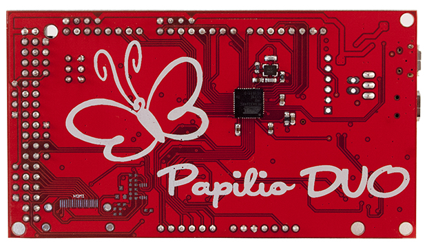
It’s been a while since we’ve seen some new boards that combine an FPGA and an Arduino, so naturally the state of the art is a little bit behind. The latest from [Jack Gassett], the Papilio Duo, aims to change that by addressing all the complaints of the original Papilio and adding some neat, modern features that you would expect on a board designed in 2014.
On board the Duo is an ATMega32u4, the same chip used in the Arduino Leonardo, allowing for easy integration with your standard Arduino projects. The top of the board is where the real money is. There’s a Spartan 6 FPGA with 9k logic cells, enough to run emulate some of the classic computers of yore, including the famous SID chip, Yamaha YM2149, and the Atari POKEY (!). With host and device USB, 512k or 2M of SRAM, and an ADC on the FPGA inputs, this board should be able to handle just about everything you would want to throw at it. There’s even a breakout for HDMI on the bottom.
There are a few interesting software features of the Duo, including a full debugger for the ATMega chip, thanks to an emulated Atmel JTAG ICE MKII. Yes, an Arduino-compatible board finally has a real debugger. The FPGA can also implement a 32 channel logic analyzer, making this not only an extremely powerful dev board, but also a useful tool to keep around the workbench.


This seems like a pretty great board. But doesn’t it seem like we should be able to do more with a microcontroller than simply emulate a game console from almost 40 years ago? Am I being unreasonable?
Actually it’s not really an emulation of a game console, but rather a clone of the console on the FPGA. But you’re not limited to mimic a game console, you can obviously do much more with an FPGA, especially in areas where microcontrollers are not suitable and ASIC are too expensive.
Right, but why is the FPGA “only” able to simulate the logic of a 40 year old console, built on something like a 6 μm feature size.
http://en.wikipedia.org/wiki/General_Instrument_AY-3-8910
“The VHDL source code is available on the Internet, and compiles to fill about 10% of a Xilinx XC2S300 FPGA.”
Not quite what the Spartan 6 FPGA offers.
“Spartan-6 FPGA family delivers an optimal balance of low risk, low cost, and low power for cost-sensitive applications.”
“Spartan-6 LX FPGAs are optimized for applications that require the absolute lowest cost.”
Prioritizing cost over performance, I guess.
Antoine: the SID , YM , and POKEY are the sounds chips only not the whole console.
Water jet: please go research what FPGA’s are and why we use them before posting further. I’m not trying to flame you , but you’re clearly uninformed.
I’ve come to the conclusion that reason that all these retro 8-bit projects exists is pretty simple.
The are made by 40 to 60 year-olds, who in their youth played Pacman at the local arcade, programmed in BASIC, learnt all the Z80 or 6502 opcodes and studied the center-fold schematics in the middle of their micro-computer reference manuals. (Yes – at one time you did get the complete schematics in the manuals!).
Now that large enough FPGAs are available and affordable, and the kids are now grown up, they can now complete their ambitions of building that perfect system using a $100 dev board, or maybe finally get to reconstruct the arcade game that ate all their pocket money.
So although the relatively tiny Spartan 6 LX9 used on this board has sixteen DSP slices that can run at over 5 GMACS and has a 100 pins that can each pump out about 1Gb/s a lot of people are quite happy to make their own 8 MHz 8-bit systems,
And why not – with one of these boards a person can now engineer a system that could outperform a 80s supercomputer [http://www.chrisfenton.com/homebrew-cray-1a/] but were is the fun in having a supercomputer?
You can implement a Z80 based computer, with VGA text display, 8K Microsoft basic, 16K of RAM etc inside about 3600 LE’s, rather less than 1/2 of the capacity of the LX9 FPGA. It’s still a pretty small device though, for sub $200 these days you can get FPGA development boards with 77,000 LE’s, 512MB of SDRAM, HDMI out, 24 bit audio in/out and an SD card socket.
you can do bitcoin mining by downloading the vhdl here
http://opencores.com/project,btcfpgaminer
What were the complaints about the Papilio – and how have they been addressed?
Adequate spacing between mounting holes and exposed circuitry was apparently not one of the complaints.
There is actually a female header partially covering one of the mounting holes and a cap on the edge of another. I’m not impressed. Have they tried to mount it to anything…… ever?
the larger SDRAM from the papilio was removed because of complaints it was “too hard” to use. go figure.
now theres a 512k sram on there instead. lower bandwidth + less space.
there’s a lot more you can do with fpgas (and even this one), but you will have to learn real verilog and spend some time slogging through digital design. fpgas have traditionally been hard to sell to the “maker arduino-blinkey light” type crowd because they are really only suited for applications that you couldn’t do with a MCU or other standard hardware.
>real verilog
or VHDL or one of the new “easier” HDLs or a schematic based HDL..
Why couldn’t they just make a “library” to make the SDRAM emulate SRAM?
They did, but it was still “too hard”. Specifically when re-using existing code that was hardcoded to use sram
SDRAM has varying access speeds. If you’d want to perfectly emulate fixed access speed of SRAM, you’d need to make it really slow and treat every access as worst case. This could mean a factor of 10 loss in speed.
I have a Papilio One I use with the ZPUino (Arduino compatible) softcore so I really like this combination. I look forward to it’s release.
I know people talk about how hard learning FPGAs is but once you start thinking of your algorithm as executing in parallel rather than serially it’s not that bad. Though I did have some experience with digital design so that probably helped on the learning curve.
Drawing an FPGA design in a graphical tool is neat, but I don’t understand why they are pushing it over actually learning a proper harware description language. Aren’t these things supposed to help people learn? A good knowlege of HDL is gunna let you do far more, far quicker than connecting wires here and there all around a clunky circuit editor.
Come now people, Verilog is not that hard! I feel they’d be doing a better service to the community by making a set of easy to use text and video tutorials.
I’ve seen horrors committed with the circuit capture tools in FPGA design, highly asyncronus designs that make you pull your hair out if you ever have to change devices or update anything, things the hardware can’t really do reliably… That being said, if done right there’s nothing wrong with the tools if you already know what you’re doing (in which case, you’re probably already using an HDL and not giving a gui tool the time of day), other than they are slow to develop for.
Either way, it’s the documentation that sells the hobby market, Arduino or not.
I believe they are pushing the graphical tool as it lowers the barrier to entry for those who would like to incorporate FPGAs into their projects but are intimidated the HDLs. After all, how many people got into Arudinos not because it’s a particularly powerful development platform but because it does the job and is easy to use?
That being said, I agree that if you stick with the graphical tools you are limiting what you can do. The time spent learning an HDL (whether it be Verlog or VHDL) is well worth it.
small steps
Where could someone with knowledge of discrete electronics start learning FPGAs?
You could try my attempt at an FPGA quickstart course that leaves out all the tedious stuff and walks you through using using most of the resources on a low-end FPGA:
http://hamsterworks.co.nz/mediawiki/index.php/FPGA_course
It is for Spartan 3E, but is equally applicable to Spartan 6 parts.
Mike thank you for taking the time to write the content for this wiki! :)