A common way to create a custom PCB at home is to do what is called the Toner Transfer Method. In this process, the trace layout of the board is printed out on a piece of special toner transfer paper that allows the ink to come off in the following step. The toner transfer paper is then put print-side-down on a copper clad PCB blank, heated and pressed with an iron. The heat and pressure from the iron transfers the toner from the paper to the copper. The exposed copper then is chemically removed, the previously applied toner protects the copper in the pad and trace areas. The toner is then removed using paint thinner.
That is a long process with many critical steps. [mlerman] wondered why no one was printing the toner directly to the PCB. He has been tinkering with printing directly on PCB blanks for 4 years now. He’s made hundreds of boards over that time and can now make a PCB in under 15 minutes.
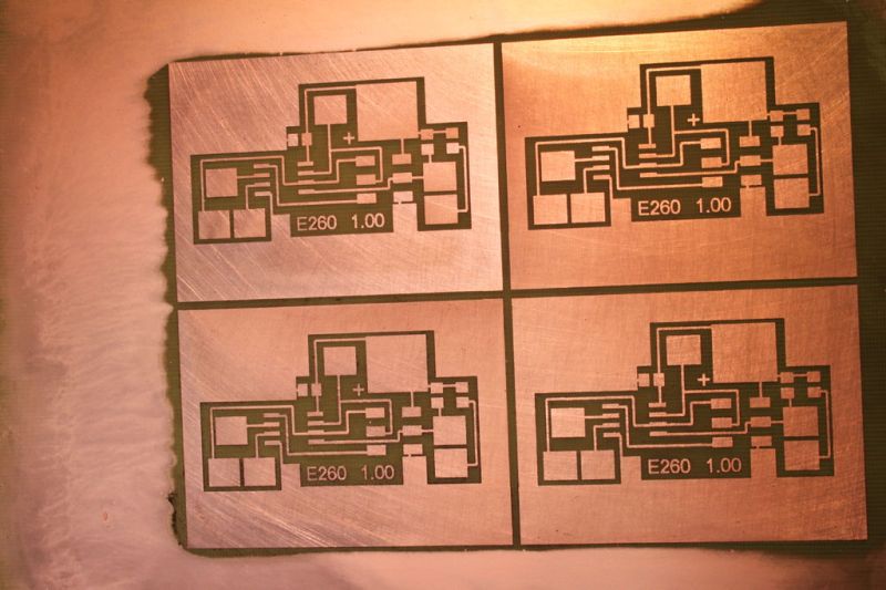
The obvious route to take would be to modify a current laser printer to accept the much-thicker-than-paper PCB boards. A few printer models were tried but [mlerman] feels the Lexmark E260 works the best due to the cost, internal mechanical components and an easily modifiable manual feed system. There is also a Local Printer Utility that allows the majority of the printer parameters to be adjusted.
As you would expect, there are several portions of the printer that have to be modified. The first is the internal paper platform which has to be clearanced so the PCB won’t run into the toner cartridge. The next part needing a change is the feeder assembly. The rubber rollers were made to grab thin paper, not thick material. To ensure a firm grip of the PCB, a second aluminum idler roller was added. It is pulled against the stock rubber roller by a spring and is essential for slip-less printing. Check out [mlerman’s] Instructable for extreme detail of all the changes he had to make to the printer.
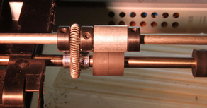
The PCB blank is not passed through the printer by itself, it is attached to an aluminum carrier. The aluminum carrier acts as a consistently-sized delivery method when using different sized PCB blanks. [mlerman] has had some great results with this setup, being able to make trace widths all the way down to 0.005 inches. Although he has made some simple two-sided boards, he wants to come up with reliable a process for fabricating more complex designs.
Thanks [Laimonas]


WHY is there not such a commercial product? I want one, now! :D
because you need to prepare pcb before printing on bare copper, and its tedious
hmmm now that i think about it – cheap printer, but gouge on ‘special pcb cartridges’ !11
There is. It’s called a laser cutter. It’s just that they cost $5,000 – $20,000. They, however, work beautifully.
http://hackaday.com/2011/09/09/laser-etched-pcb-production/
and http://hackaday.com/2008/08/03/laser-etching-printed-circuit-boards/ for methods of doing this less expensively with a RepRap and then how to do it with an Epilog.
And lastly, here is a commercial galvo laser for comparison.
http://www.youtube.com/watch?v=n29LrMF8LC4
It looks like that ablative laser system starts at $140,000.
I’ve not had much luck burning away spray paint with a laser engraver (“cutter”), because it leaves a soot that has to be wiped away with a solvent, and that risks wiping away the traces you want left behind. I didn’t think to try flat black, I think I had a semi-gloss or glossy. The articles didn’t say what kind of spray paint they used, I think I used an acrylic enamel.
I wonder what the running cost of the machine is, what would it cost to have a 5x5cm double sided board made.
If someone in EU could make me 1 copy of a 5×5 for $10 and then ship it so that I can have it at home in <5 days that would be great. I would prefer this service in place of all the chinese manufactures.
You can buy a new 40w CO2 desktop laser cutter for as little as $425 off of ebay.
Well, they are cheap, but unfortunately they don’t cut through copper on PCB, there is a reason why the LPKF needs 1.4 kW mains input. Anyways when cutting metals it would make more sense to use YAG based lasers, cause they produce wavelengths witch will be absorbed better by metals, CO2 suits well for cutting organic materials. You can cut metals with CO2 but just need more power.
You could ditch the original optics and replace them with a fast pulsed YAG, most parts to DIY one could be had for about $500 from ebay…Not too sure about the dielectric mirrors (pretty much the only type of mirror that will survive the 100s of kW during the pulse) though, they are fairly expensive and you need at least 2 of them plus a final focusing lens for the head…also, it would be fairly slow when compared to the $140k one, but then again for a fraction of the cost.
Emma; It will work if you use it to expose the board for etching, rather than hoping it cuts copper. Koit is right, CO2 lasers need to be much higher powered to cut copper. Your fiberboard edges and surfaces will be terrible.
I have an Epson Stylus printer that I’ve been thinking of using for PCB’s. After all, it can print directly on CD’s and probably won’t need any modification, and I think others have done it before…
http://www.fullspectrumengineering.com/tutorial.html
“special toner transfer paper that allows the ink to come off” – you know what grinds my gears? Calling toner ink. :)
Also “special toner transfer paper” meaning the cheapest, tackiest magazine page you can find around the house
I’ve tried that cheap magazines and it was a nightmare. On “special toner transfer paper” I can do 8mils traces with 10mil spacing very reliably, but this requires that copper is polished first.
I’ve gone the magazine route with some success. (I think high clay content in the paper is the key.) But my results are much more consistent using transfer paper and toner foil.
i tried magazine paper once…
It adhered to the Photo Transfer roll of my Printer, and was winded around it.
It was a financial total loss, as the Paper was shredded to bits by the mechanism, that scraps residue Toner of the roll.
@admin: sorry, didnt mean to press report :-(
it seems to depend on the printer youhave, the cheaper printers dont embed the toner into the page that well, I know a chap who was able to sue ANY paper to do toner transer, worked perfect every time. go figure.
It’s actually about the toner itself, there are more types of toner, main difference being in the binder agent. Some use thermoplastics (that’s the one you want), others use resins (bad for transferring)…
What sucks though, is that manufacturers almost never even give a hint which binder the toner uses, making “the right choice” a hit and miss affair…
Perhaps printing on sticky back copper foil might provide a solution to the thickness issue.
stick on copper foil sounds like a good idea to me though presumably the adhesive would need to be reasonably resistant to the etching, in which case the new board would have sticky bits between the copper.. Hold on, that could be REALLY useful when positioning components, especially surface mount!
The copper surface is on top of the adhesive, so your parts are raised by that thickness.and not touched the adhesive layer. You really don’t want that type of goo on your parts or worse on your solder joints.
The regular copper tape adhesive melts when you solder on top of it. The tape itself would slide around on the now liquidifed glue. I have done it a lot of times to make a copper power plane for modding high speed boards.
You really need a high temperate adhesive (cured) to handle soldering temperature.
This post should probably mention that the fuser was taken out, so you still need to dig out your iron to melt the toner in place.
Still, a great way to get around the transparancy step. I wonder how many error messages he had to get through when trying to do this? I’m now on three with my Epson Inkjet PCB printer mod and I haven’t got through the startup sequence yet. Service manual would sure be helpful, perhaps that’s the best reason to go for Laser instead of Inkjet.
No heat needed, he uses acetone vapor to fix the toner onto the PCB, neat!
Special paper?
I just use reasonably thick shiny magazine pages.
Cut out and stuck to copy paper to make it feed properly.
I’ve been using the glossy copy paper they sell at Fedex/Kinko stores (about $15 for a ream of 500 sheets IIRC) and it works great.
Oh, and an unmodified a4 laminator to transfer the “toner” to the board.
Done many double sided boards this way.
it’s a pretty commom hack in brazil.And for those who still use special paper or magazine paper commom printer paper work to pcb too.
I wonder if you could print a copper based compound instead of toner/ink. Then through some reduction process leave the copper deposited on the substrate. Actually even free standing copper could be interesting for SMD boards.
I mean onto a blank fibreglass board with no copper on it already. Basically can the etching stage be skipped, through some chemistry. And maybe even with some less noxious chemicals.
You can print with the traces with conductive ink ( http://www.methode.com/sensors-and-switches/conductive-and-resistive-inks.html#.VDvJ_Bbjbis ) and then use galvanic process – with copper-electrolyte – to add copper.
Easier / faster? I’m not sure.
You could technically use vapor deposition (or magnetron sputtering), but that requires high vacuum to work reliably…it would however allow you to deposit a layer of copper on almost anything :D
Whatever conductive compound + adhesive you have initially deposited on the FR4 would have to withstand soldering temperature and both still stick to the FR4 and copper. Also it cannot out gas under heat.
Not fun if your fine tracks peels off when you try to solder/reflow the board.
Wow. Very thorough instructions and a decent parts list up front. I literally purchased a 260d some time ago specifically for doing toner-transfer. If this wasn’t the only working printer in the house right now I’d be duplicating this hack in a heartbeat!
I wish I’d have the time to follow my ideas… That was one of the first thoughts I had when I read about the toner transfer method…
Video from Mark L.
https://www.youtube.com/watch?v=VY-7hQ6ocx8
I used the toner transfer method for some time, and also thought about modifying a printer to print the toner (or etch resistant ink) directly on the PCB. In the end, however, I ended up building a small, cheap and simple UV exposure box using blue/UV LED’s. I couldn’t be happier with the quality of the boards I can produce and how easy it is.
I think this is a great idea. I thought about it many times as well, but since I also used my printer for regular prints i did’t do it. Also, it is perfectly feasible to get very good results in 15 minutes as well, and on the cheap. While you can use special paper, some magazine paper works excellent. Once i found one, i used the same for years, you can get lots of PCBs from a 100 page magazine.
Time breakout is like:
-3 minutes to cut the pcb + smooth edges
-2 minutes clean pcb
-2 minutes print + stick pcb to page
-2 minutes iron
-2-3 minutes remove paper
-2-3 minutes etch with sponge method
He’s got my attention! I’ve been using toner transfer with vinyl shelf paper for some time now.
The reason nobody did it was because of the question on how you get a piece of copperclad material to work on a roller-based static charge transfer system. Because copper you might be surprised to learn is very conductive.
MTE. A laser printer works by creating a static charge on the paper, which then attracts the toner. I would expect the charge to immediately dissipate through the copper.
Try printing traces directly without etching. http://www.cartesianco.com/
It is web scam only, nothing real.
Hello! Is the LEXMARK E360 the same as a E260? Can it also be modified?
wow…its really awesome…..
Its really awesome