For a few years now, the Rigol DS1052E has been the unofficial My First Oscilloscope™. It’s cheap, it’s good enough for most projects, and there have been a number hacks and mods for this very popular scope to give it twice as much bandwidth and other interesting tools. The 1052E is a bit long in the tooth and Rigol has just released the long-awaited update, the DS1054Z. It’s a four-channel scope, has a bigger screen, more bells and whistles, and only costs $50 more than the six-year-old 1052E. Basically, if you’re in the market for a cheap, usable oscilloscope, scratch the ~52E off your list and replace it with the ~54Z.
With four channels of input, [Dave Jones] was wondering how the engineers at Rigol managed to stuff two additional front ends into the scope while still meeting the magic price point of $400. This means it’s time for [Dave] to reverse engineer the 1054Z, and give everyone on the Internet a glimpse at how a real engineer tears apart the worth of other engineers.
The first thing [Dave] does once the board is out of the enclosure is taking a nice, clear, and in-focus picture of both sides of the board. These pictures are edited, turned into a line drawing, and printed out on a transparency sheet. This way, both sides of the board can be viewed at once, allowing for a few dry erase marker to highlight the traces and signals.
Unless your voyage on the sea of reverse engineering takes you to the island of despair and desoldering individual components, you’ll be measuring the values of individual components in circuit. For this, you’ll want a low-voltage ohms function on your meter; if you’re putting too much voltage through a component, you’ll probably turn on some silicon in the circuit, and your measurements will be crap. Luckily, [Dave] shows a way to test if your meter will work for this kind of work; you’ll need another meter.
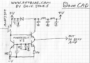
From there, it’s basically looking at datasheets and drawing a schematic of the circuit; inputs go at the left, outputs at the right, ground is at the bottom, and positive rails are at the top. It’s harder than it sounds – most of [Dave]’s expertise in this area is just pattern recognition. It’s one thing to reverse engineer a circuit through brute force, but knowing the why and how of how the circuit works makes things much easier.


Dave Jones a ‘real engineer’ ?
As someone pointed out on here a while back, this is a ‘man’ who is incapable of recognizing a simple full-wave rectifier when he sees one. Something which even a first year student should be capable of.
Are you implying he’s not really a man?
Dave is obviously a cat masquerading as an Electronics Engineer
Nope. He’s a semi-hysterical Aussie. An entirely non-human form of life :)
Indeed.
It’s life Jim, but not as we know it :)
Negative. He is a meat popsicle.
I reckon he falls into the “he’s forgotten more in his lifetime than you’ll ever remember in yours” category, at least for most of us. I’m not going to bitch about whether or not he might make the occasional verbal misstep, I’m going to try to learn from what he’s saying… the man’s lightyears ahead of most, and even that might be selling him short.
I remember that one, the braun toothbrush, but it’s not the only “verbal misstep” he’s made. Not by a long way.
His fundamental lack of the most basic knowledge of circuit analysis is blatantly obvious to anyone who has studied the subject formally. In fact it’s usually the very first thing you study.
As for the “forgotten more” nonsense…
Electronics is far too vast a field for anyone to have more than a general knowledge of it except in their specific area of expertise. That’s why the fundamentals such as circuit analysis are so important and why formal courses place so much emphasis on it.
However it isn’t just him. Far, far worse are the drooling idiots who follow him religiously, right or wrong. Just look at some of the comments they post on his blog. These people really shouldn’t be allowed access to tools. Or any sharp object for that matter.
Sadly, as others have pointed out almost every time the question of his competence has come up.
EEV Blog really is one of the very few such things , even if it is presented by a semi-hysterical amateur who’s somehow managed to avoid electrocuting himself.
Just don’t take everything he says at face value. A lot of it is not entirely accurate and some of it is just plain wrong.
Full Disclosure:
I have degrees in Computer Science and Electronic Engineering, plus the usual double handful of industry specific qualifications.
Not everybody knows these references, like the “braun toothbrush”. Why do some people think David Jones isn’t such a great engineer? Links?
They are referring to the Braun Electric Toothbrush Teardown posted on EEV blog some time last year (a search for ‘eev blog braun’ should find it).
The ‘power supply’ is a ‘split’ transformer with the primary winding in the base unit and a centre-tapped secondary winding in the base of the toothbrush. Two diodes provide full-wave rectification with centre-tap as GND (0V).
It’s a fairly standard configuration for this type of cordless appliance. Cheap, easy to manufacture and pretty reliable, Cheap… Yes I know I mentioned cheap twice but it bears repeating :)
“Why do some people think David Jones isn’t such a great engineer?”
That’s a bit more subjective. I’d guess it’s mostly the one’s who sweated blood to get their qualifications and wince in pain every time he comes out with a blunder like this.
Consider how many times you’ve sat watching something on TV only to hear someone come out with the most ridiculous drivel in connection with technologies they obviously have absolutely no understanding of.
Painful, isn’t it?
In this specific case it’s such a basic power supply circuit that he really should have recognised it.
Ah, I see what you’re saying. This occurs at about 19:30 in the video.
The way I see it, yeah that’s an extremely basic circuit that I know is taught at sophomore year at my college, but it doesn’t convince me that David Jones is such a bad engineer.
His confusion could come from the fact that he drew the circuit retarded-ly, with the “2nd” coil coming up from the ground point instead of down, how a center tapped coil is normally shown.
Later on though, he does correctly state it is a full-wave rectifier at 28:30.
In any case, perhaps David Jones is the “Edison” type and not the “Tesla” type of brain. I’d need to see more blunders and worse blunders than that to think he’s a “bad engineer”.
Im not sure I get what the problem here is.. What did he mis-state?
Yeah the drawing is a bit wonky compared to how that transformer is normally drawn, but it is just as good of a representation as the other. I mean.. takes a second longer to recognize it.. but the center tap is clearly ground, and the two “outputs” clearly pass through diodes and then are tied together. This is obviously full wave rectified.
If the complaint was referring to when he says “I dont know why they have two coils here..” well that could just as easily have been a single coil. I agree that his follow on is not very well stated.. but they could have used one or two coils. Two costs more, and is more efficient, but the circuit could have been designed to work with one. So, his statement is technically an accurate one.. if you read between the lines “I dont know which particular parameters they were designing for which drove them to chose a two coil configuration. Cost, performance, simplicity, or some other parameter.”
I didnt read into it as “I have no fraking idea how this thing works or what it is” which apparently is what some people are thinking?
I’m almost on the same page. I’m actually appalled by the lack of tact he displays and more shocked that the people find this to be a sign of professionalism.
He does not like criticism and he will moan everytime someone says (rightly) something about him.
I hate how he treats the packages and judges the people: “he’s a smoker”, “he has a cat”, “he is religious”, etc. I’m atheist and probably non-‘cat lover’ as well but I would never say those nasty things he said to an audience.
But actually the worst thing in my eyes is the superficiality. You cannot keep track of how many times he says in a video ‘I cannot be bothered with that’, ‘you have to do the research yourself’, ‘not worth doing’. Contrast this with Mike’s (mikeselectricstuff) approach. And now Dave would probably say something: ‘yeah, but I have a family and job and forum, and blah blah, I cannot be bothered’.
I still watch most of his videos, though unsubscribed and at 1.25-1.5x speed
Ok, enough with the rant, just had to get it off my chest.
Uh, you mean the guys that may be electrical engineers themselves? Or electronics techs that tend to know waaaaaaaayyyyyyyyyyyyyyyyyyyyyy more practical things about electronics than most engineers?
I know a sad number of EE’s who actually know dick about actual electronics because they are only good at math and theory, if even that. But hand them anything “real” and look out, cause sparks will probably fly and you may have the teach them which end of the soldering iron to hold…
If I had advice for anyone going to school to be an EE it would be: Labs and reasearch projects are your friends. Don’t neglect real world, hands on work or hobby projects to gain some practical insight. You will thank me later.
As a sophomore EE student I can say that this is so sadly true. All the students around me seem to do so well in the classroom/lecture setting, but are completely lost when we get into the lab. I am the complete opposite. I don’t do the greatest on the written tests, but in the lab I seem to do far better, even though I “know less” because my grades aren’t the best.
I too am just like you. From someone on the other end of that road, the practical experience and intuition/feel for what is going on will go pretty far. I wish I had studied more on the analysis stuff, but book study is a thing you can pick up again any time you NEED it.
PROPER soldering techniques, the ability to lay up a complex circuit on prototyping boards, and whacking together something that just works, or demonstrates the overall idea of the project is incredibly useful. Good at nose in book is the opposite of useful.
Know how to look up and confirm or correct your understanding of the theory. As you go along, you will naturally put a lot of stuff you don’t use regularly in your current line of work into the back of your head anyway. But you still need to study enough that you can recognize patterns and how to look up the equations.
@arbartz grades are not a measure of knowledge, so don’t let that get you down. Being able to do the labs is worth much more than the classroom portion, but if you understand the workings in the lab it should make the classroom more intuitive.
When I was majoring in EET I had a few friends that were EE majors. One of them once asked me “what does a diode actually do? We’ve been learning the math on them for a month but what does it do?” I was amazed.
“We’ve been learning the MATH on them for a month, but what does it do?”
I cannot even begin to explain how many times I’ve heard things along these lines…
yeah yeah! And, I had found that a lot of the circuits we were asked to analyze were the EE equivalent to high school math story problems. Not all.. but many. Demonstrate that you know the math, while at the same time demonstrating no practical application of it. Resistor spaghetti networks. I can only have so much fun reducing them down to one. Parallel resistance rules of thumb ARE pretty useful in a quick and dirty prototyping situation though. “Ok.. Ive got 2 x 1K and a 500 ohm resistor here.. If I whack them all in parallel I get 500 from the two 1K, and 500, which gives me about 250 ohms. That’s a shitty way to get a 220 ohm resistor, but.. it is what it is.”
That reminds me of when I was in my 2nd year of a 2 year EETN program at college and one of my lab partners for a project didn’t know how capacitors worked. The rest of us looked at him and asked “How exactly did you pass first year?” as we had spent a whole semester working on capacitive and inductive circuits. 0_o
I find him to be talented, entertaining..and a good engineer.
I’m mostly a software guy…I wish I knew half what he does about electronics.
Go Dave,,,Go EEV Blog :-)
Amen
Printing out the sides of the boards only woks with double sided PCB, once you go to 4 or greater layers with blind/buried vias you are well and truly stuffed.
Unless you have a friend working with an MRI machine and some spare time……
Meh, 4 you can manage, usually. Layer 2 and 3 are usually just planes, and with a strong light you can usually make out the layer splits. 6 and up, though, yeah, screwed.
If you don’t mind destroying the circuit, sand off some, take a pic, sand off some more, take a pic, until you reach the top and everything falls apart.
there are RE houses that will do it for you, I remember links to russian and chinese ones somewhere, to lazy to search now.
Bad advice… You could seriously end up in a world of shit for exporting things that are illegal to export. And I’m sure both of those countries would welcome any hardware to reverse engineer…
There are even places that do this with CHIPS
I have done my share of tracing double side PCB with through hole parts in the old days. With SMT parts, it is pretty to pop a PCB in the toaster oven and literally scrape the parts off. A bit more work with a hot air tool if you want to measure the individual passives values. :P
Guys that work on reverse engineering and making firmware desolder all the parts off boards to trace the circuits. e.g. Rockbox, Dockstar, rt5350f routers etc.
Flat bed scanners are very nice for taking pictures of PCB without the usual distortion with cameras and scaling are easily repeatable. If I had to do one, I would photoshop the two scans and play with transparency setting so you can see them super-imposed.
Most of the time you don’t need to do the whole thing unless you are cloning it. You’ll just need to figure out the part you need.
I tried using a flat bed scanner (or was it a photocopier?) a long time ago for reverse engineering a board but the thickness of the components put the PCB traces badly out of focus. Do you have to depopulate the entire board before scanning (which would suck) or do some scanners just work better than others?
CIS (Contact image sensor) scanners are not suitable for scanning non-flat objects. I guess that tekkieneet scans where made with a CCD-based scanner. Most (if not all) cheap scanners nowadays use CIS technology and you won’t be able to scan a PCB with them.
I found my old scanner in Goodwill. hp didn’t bother updating their XP driver for Win7 x64, so probably why it was there. That’s should tell you how old it was. The scan head on mine is different. There is no integrated lens on top of the sensor.
http://en.wikipedia.org/wiki/Contact_image_sensor
I had done board scan on photocopiers at work years ago with similar results. Unfortunately no colours nor scanned image. Highlighter works good on the scans for marking parts and traces for rework. Surprising they also work marking actual passives. :)
Saw a couple of scanners at goodwill yesterday. One hp combo scanner/inkjet photo printer and a Canon LED based scanner. Now I know what I should watch out for. Thanks [Michal].
http://em.motokokusanagi.com/web/Misc%20Electronics/Router/Linksys%20BESFR81/
FYI: These are the scans of the old wired Linksys router on my old hp flatbed scanner. FYI Samsung ARM chip is 0.5mm pitch in first picture, so I am guess the tracks would be 7-8 mil range. I’ll let you be the judge of the focus and picture quality.(untouched except for cropping)
There are tall components – Ethernet RJ45. My camera would not be able to take that without have lots of lens distortion for a large PCB in macro mode.
The firmware got bricked and stopped working. So I reverse engineered enough of it to have the mainboard works as an unmanaged switch. (I put in I2C EEPROM and a crystal for the uplink port which prevents the switch from rebooting over and over) For that two boards, I actually just use my DMM continuity check to map out the expansion connector as I have datasheets for all the parts. I used a conductive foam to initial narrow down the rough location of the signal I was searching before going pin to pin.
I haven’t done much for the ARM chip as you can now buy eval board with much better open source support and speed than old ARM7 chips.
One other thing you can do with the image of the PCB after scanning that is useful in RE – is to play with the color settings (or reduce the palette) so that the traces are a mostly or completely single color. Then flood-fill the trace from a pin on one part to see where it goes (to another part or a via or such).
Mainly useful for single and dual-sided boards; I used this technique a long time ago to trace out pins from a super-i/o chip on a 486 motherboard (that was custom built for a set-top box – and used an AMD 586/133 for the cpu) in order to find out where a serial port and other ports that didn’t have headers could be used.
Check this video on youtube on how to unlock all features and make the DS1054Z into a 100MHz Oscilloscope:
http://www.youtube.com/watch?v=NmJNOwcJh7Y
Now, I’m far from as capable as you guys and couldn’t find a satisfying result with Google.
But WHAT do you guys actually use an oscillator for ? I just cant think of a proper purpose for it.
ask your mo… nah, too easy
are you serious?
http://en.wikipedia.org/wiki/Electronic_oscillator
Wow you linked Wikipedia, which totally shows examples on how someone would use it !
Thanks for nothing.
An oscillator is a timing element – for example there is an oscillator in your wall clock or mechanical wristwatch. It runs at 32.768 KHz. This number is divided down by a 15-stage counter, which will give you a pulse/signal exactly each second.
Never noticed that was the reason for the 32.768KHz before. I know that 2^15 is 32768 but I never made the link before, thanks.
Where would we be without synthesizers in bands. Synthesizers are collections of oscillators plus a keyboard just as a piano is a collection of metal strings with a keyboard.
How about a local oscillator for mixing down RF to IF? And you pretty much have to have an oscillator of some sort to genreate the RF in the first place.
Clocks and timing of course for digital circuits and microprocessors
Oscillators are perhaps the most important circuits in electronics, really.
“Oscillator” or “Oscilloscope”?
Yeah, it’s not clear, but given the context of this HaD post, it seems like oscilloscope might be the subject of the question. Anyway, an oscilloscope is used for displaying the time variations of a voltage or other electronic signal. One common use is to view the output of an oscillator. And oscillators are used to make circuits do things that change over time. Sending and receiving radio waves, making music or other sounds, sending data over transmission lines, these are but a few examples of the kinds of things that use oscillators. Every electronic device more interesting than a flashlight contains at least one oscillator (wait — I just remembered that my dimmable LED flashlight has an oscillator that controls the brightness by doing PWM).
Rather than this quite involved ‘manual’ method I used a digital method.
1. Take the best photos you can take, flat (non-distorted), at 35mm equivalent, no reflections. It will save you a ton of time afterwards
2. Do the same for the other side. You might need to remove larger components.
3. Import both pictures as new layers into GIMP. Mirror one side.
4. Align them to be straight on the sides, adjust the perspective on all corners so they are squared.
5. Set the transparency on the top layer to ~20% and adjust one of the layers match with the registration marks/holes/vias on the other layer.
7. Profit
BTW see my link a few post up for flat bed scanner pictures. Old $10 hp scanner from goodwill beats the heck out of my 3rd gen digital camera. I haven’t even crank up the resolution.
you need a really old, LPT driver scanner to do that, new ones will simply blur
It (hp 4470c) is new enough to have USB + LPT + Apple Talk (!?). It is a pain to have to run XPMode to talk to it, but very useful for my hardware pictures.
Would be really nice if someone reverse engineered this (or one with similar performance) frontend properly, and released it as open hardware. I would gladly buy that module with 2 inputs at ~$50.