There are two printers being shown off at the 2015 Consumer Electronics shows which really spark our interest. They are the Voltera and the Voxel8. Each is taking on the challenge of printing circuits. They use similar techniques but approach the problem in very different ways.
Voxel8
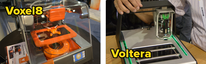
![[Michael Bell] poses with the Voxel8](https://i0.wp.com/hackaday.com/wp-content/uploads/2015/01/dsc_0405.jpg?w=530&h=353&ssl=1 "DSC_0405")


The Voxel8 marries the idea of a 3D printer with a silver conductive ink dispenser. You start by modeling your entire design, hardware and electronics, all in one. The printer will then begin the 3D print, pausing when necessary for you to add electronics and mechanicals. With the parts — and their pins — in place it lays out the conductive ink to connect the components and then continues with the 3D printing to finish the object.
Voltera
![[Alroy Almeida] poses with the Voltera](https://i0.wp.com/hackaday.com/wp-content/uploads/2015/01/dsc_0432.jpg?w=524&h=350&ssl=1 "DSC_0432")


The Voltera is a PCB printer that uses silver conductive ink. It prints the ink onto a substrate. Pads made of the ink are used to solder the components in place after the printing is finished. The trick added to this design is the ability to print two layers, both on the same side of the board. There is a second ink material which is an insulator. It is laid over the first conductive layer before the second is printed, allowing traces to cross over each other.
Congratulations to the Voltera team who won $50k from the 2015 Hardware Battlefield at CES.
Our Thoughts
We didn’t see enough to shake our skepticism about the viability of silver conductive ink to take the place of copper on prototype boards. But if anyone is going to make the case that it is plausible these two offerings will.
One interesting thing about the Voxel8 is the ability to specify point-to-point wiring as a “part”. If you do so, the machine will pause while you solder the wires in place before it encapsulates them with the rest of the print. Of course if you’re going to do this manually it shouldn’t really matter which printer you use for it.
What do think about the future of conductive ink for prototyping? Lets us know in the comments.


Have either published specifications on their trace resistances?
Silver conducts better than copper:
Electrical conductivity
(10.E6 Siemens/m)
Silver 62,1
copper 58,5
Except the print is not a solid piece of silver wire… They are more like granular silver in a paint emulsion, so the resistance can be significant.
If its anything like the silver conductive ink it’s a lot worse than copper. I guarantee these are not printing in even 50% copper at the 1200 degrees needed for such an alloy, even if they were printing in Solder, that means 700 degrees and the PLA will start to burn right away.
I’ll take them seriously by the time they become affordable to the point that they are actually a competitively viable technology. Soooo…. probably when whatever patents they filed run out :P
I don’t see this catching on with silver ink being so expensive and all the board “printers” coming out. It’s more of a novelty than a viable product. That and board houses like OshPark are so cheap and easy and give vastly superior results.
i saw the video of the voxel 8 on their website, it looks cool and all but is only good for “disposable devices” i’d say, unless you make them open frame, because what happens if you place the wrong chip? or a part burns out like a cap? how do you replace it if you make the whole thing inside a 3d printed frame that can’t be opened? every design would have to take this into account, but the designers at voxel8 didn’t take any of that in account, the models i saw where placed inside a solid 3d printed model that can’t be open, that’s why i say it would only be good for “disposable devices”, and there’s also the factor that r4k pointed out, what about resistance? what if i want to build something that involves AC? this printer is pretty and all, but too many factors left aside
Well.. if you achieve the Reprap dream of cheap, self-reproducing make-everything machines for everyone then that doesn’t matter so much. Just print a new board cause it’s cheap.
Recycling the raw materials of the old board might be a challenge though.
Back in 2009 at a conference (ISMRM) I saw a talk where a group “printed” radio frequency probes (essentially tuned magnetic field loop antennas) for MRI using a silver based ink in a very expensive inkjet printer. Once printed the substrate (FR4, kapton, PTFE for example) was baked in an oven which solidified the ink into a contiguous conductive surface. The results looked good, the probes performed as well as a regular copper trace coil, where low resistance is crucial. However this baking process was important. Unless a high temperature 3d printing material is available then this will not be possible, and these printed electronics will be only possible for very basic circuits where low resistance lines are not necessary. Maybe they have cracked it though, but I’ll believe it when my multimeter sees it. Also a hacker friendly circuit needs to be able to withstand re-soldering multiple times…
Back in 2009 at a conference (ISMRM) I saw a talk where a group “printed” radio frequency probes (essentially tuned magnetic field loop antennas) for MRI using a silver based ink in a very expensive inkjet printer. Once printed the substrate (FR4, kapton, PTFE for example) was baked in an oven which solidified the ink into a contiguous conductive surface. The results looked good, the probes performed as well as a regular copper trace coil, where low resistance is crucial. However this baking process was important. Unless a high temperature 3d printing material is available then this will not be possible, and these printed electronics will be only possible for very basic circuits where low resistance lines are not necessary. Maybe they have cracked it though, but I’ll believe it when my multimeter sees it. Also a hacker friendly circuit needs to be able to withstand re-soldering multiple times…
Unless these guys have some game changing ink tech (which I think they would be VERY clear about) the resistance of these materials is 2-3 orders of magnitude higher than solid copper traces (?x10tothe-2 ohms/square vs ?x10tothe-5 Ohms/ square)(sorry for my lack of superscript-fu). The difference has real effects on circuit design. I notice both demos show fairly high voltage/resistance insensitive applications.
It is also important to find out what the trace resolution and/or accuracy is on these machines, .03 cm is acceptable as a wall width but is hopeless for even a lot of through hole(much less SMD) components.
FYI you don’t need super script fu. You just need a ^ or and E Both 10E-5 and 10^-5 are legitimate ways of writing what you’re trying to say.
Actually, it is 1E-5 or 10^-5. 10E-5 would be 1E-4, as E could be replaced by *10^.
http://en.wikipedia.org/wiki/Scientific_notation#E_notation
Unless you’re an engineer, in which case 1E-5 is more commonly known as 10E-6 or 10u (because nobody can remember the code for µ).
Thanks to google, I found out that the ink used is probably DuPont 5021 (It perfectly matches the sheet resistance given on the voltera site). http://www.dupont.com/content/dam/assets/products-and-services/electronic-electrical-materials/assets/datasheets/prodlib/5021.pdf
Since I had never heard of sheet resistance, I could not tell whether 20mΩ/sq was a good or bad value. So some more googeing resulted in this: http://ftp.icpdas.com/pub/beta_version/2012%20ADI%20Tech%20Day/Mix%20signal%20Layout.pdf
Apparently 0.48mΩ/sq are the sheet resistance of a standard copper PCB.
In conclusion, the values given by you are spot on. The tech doesn’t seem that game changing.
If you have a track 10 mils wide and 1″ long, there are 100 [10 mil x 10 mil] squares.
The silver track would be 100 squares x 20mΩ/sq = 2 Ω.
The copper tack would be 100 squares x 0.48mΩ/sq = 0.048 Ω
2 Ω can be a problem if it is for routing power. At 100mA, that’s 0.2V drop.
One thing that is being forgotten is the height of the trace. Typical copper clad boards have an approximate thickness of 35 microns (1 ounce)
The resistance values on our site are for a 25 micron trace height. However our traces are being printed at a 100 microns or higher. This means the effective sheet resistance is ~5mOhm/square.
Closer to launch we will clean up the website and publish clearer information regarding the trace resistance. (And of course put up some more pictures)
Jesus Zozaya
Voltera Cofounder.
Using the 5mΩ/sq figure, a track 10 mils wide and 1″ long = 0.5 Ω.
Hi tekkienet – just wanted to let you know that we’ve published some videos on track resistance on our kickstarter campaign
http://kck.st/1M9mVB0
It looks amazing to start with.
Here are my questions:
– How do they maintain temperature for reflow while environment is open?
– What is the accuracy of paths?
– Can they print for small smd foot prints like chip with 100 pins?
– And no hole on pcb
– And finally how much their machine cost?
The Voxel8 is 9k, the other one doesn’t say.
Found a video where the price of the Voltera is stated (at ~8:50): http://techcrunch.com/2015/01/06/the-voltera-v-one-makes-circuit-boards-in-minutes/
Apparently, it will be $1499 for the kickstarter with a 60% profit margin and then it’ll go up from there.
They’ll go UP from a 60% profit margin? Man, fuck businessmen these days. If engineers ran companies, things would be so much better.
They are not producing a commodity. They are developing products in an entirely new industry. They have to recoup their investment in the research, design, and development. The actual cost of the hardware is probably very small compared to their sunk costs.
Hey guys – just wanted to let you know we’ve launched on Kickstarter this week
Hi tekkienet – just wanted to let you know that we’ve published some videos on track resistance on our kickstarter campaign
http://kck.st/1M9mVB0
I watch a video presentation on youtube where they said the voltera was 1500$, with the possibility of letting one cheaper through their kickstarter project.
Can confirm, there will be early bird units.
I encourage those interested to sign up for our mailing list to be the first to know when we launch.
Jesus Zozaya
Voltera Cofounder
Everything explained in their web site (link in article). Price tag is scary though ($9K)
Ink tech? Why not say solder, because that’s what it is essentially. There is no ‘ink’ in these printers.
It IS an ink, though. Silver particles floating in some sort of carrier. If it were me, however, I’d be using solder paste in these things…not sure why they aren’t…
Then what? Stick it in a reflow oven? The whole thing would melt, not just the solder!
Problem is that your paint has to also stick to the substrate material. That’s what the binder does. http://en.wikipedia.org/wiki/Paint#Binder_.28or_film_former.29
With just solder on say bare FR4 surface, it’ll just for a ball of solder because of surface tension and not a track or whatever you want to form.
I look forward to hearing about your CastAR experience. I had a really good experience with the hotglue prototype Jeri was showing off at a pub in SF, and then I had a really bad experience with a polished looking pair at last year’s Maker Faire.
It doesn’t drill holes. That’s essential. Lots of parts are only through-hole as are connectors, vias, etc. Many ICs have ground pads underneath. The pads must connect to a bottom layer with vias for heat sinking and electrical. Many boards simply cannot be routed without vias. Multilayer printing introduces height variations which make the board unsolderable. There’s no hint about peel strength, thermal conductivity, temperature range, trace cracking, rework, solderability, long-term performance. Shelf life of the ink? Cost of the ink? I don’t want a board that stops working in two months or fails when flexed a little. I don’t want a company that disappears in 6 months and leaves me with no source of expedables. The ink is special and sole-source.
This would do 10% of my prototypes. Milling can do maybe 25%. Sending a board out for fab does not cost hundreds. It costs typically 20 bucks for a small board. Another toy by twenty-somethings with no experience in the real world. They’ll sell a few units and the company will disappear.
Low sheet resistance, comparable design rules (8/8 or better), coplanarity for SMT part, soldermask, power/ground plane, controlled impedance traces are essential for it to be an alternative for PCB proto.
Here’s a thought: what about adding ‘trenches’ to the print, then placing copper wires bent to the proper shape with a miniature DIWire?
I remember very little about it, but there was a process developed in the 1970s, that was kind of a hybrid between printed circuits and wire-wrap. It involved robotically running insulated wires point-to-point on the back side of a fiberglass-epoxy substrate and tacking them down along the way with an adhesive. Many layers of wiring could be done. I don’t remember how the terminations were handled – whether the insulation was heat-stripped or what – but I think the wires were robotically soldered to the component leads.
This would be a little different if implemented today, since surface mount components would change the termination method for sure. But think about this: if you “dead bug” BGA components (i.e., mount them ball-side up), you have access to all of the pins and don’t need high-priced soldering systems.
Now put this together with 3D printing, and you can print the basic board with wells for the components so the “wiring robot” can run wires on top of components. It’s kind of an inside-out version of a multi-layer PCB. Printing wells for the components also lets you build prototypes without a pick-and-place machine; a pair of tweezers are all you need because the substrate holds the components in place.
As with other additive manufacturing techniques, this would probably be slower and more expensive for high volume than multi-layer PCBs, but could be a big improvement for rapid prototyping, both in cost and in turn-around time.
You are thinking of Multiwire… it’s still available: http://www.pcktech.com/dwirs.htm
Yes, that’s it! But it looks like they sold the works to Hitachi Chemical, who illustrates it a lot better here: http://www.hitachi-chemical.com/products_pwb_05.htm
what problem are these two companies actually solving?
They are certainly not (yet/) improving the pcb toolchain as their product is miles behind what you can get from a pcb house. Milling a board yourself gives better results too, probably.
They forego the pcb, but they do not make clear why that would give better results, or even how to design your circuits for such a scenario.
I fear the problem they really are solving are unparted fool-money combinations.
Both appear to be attempting to solve the hobby/DIY electronics problem: point-to-point wiring by hand is tedious, error prone, and unreliable, but PCBs are expensive and take a lot of time, whether you’re making them yourself or buying them from a fab house.
NOBODY is really happy with PCBs, since even in large quantities they are expensive, and making even the most minor circuit change takes weeks and turns your current bare PCB inventory into scrap, so even though printed electronics is certainly not ready for mass production, as the technology advances what we can look forward to are circuit changes that can be made in a day, and zero inventory for product-specific circuit boards. Most manufacturers, even those who do pick-and-place and soldering in-house, currently farm out their PC boards because PCB fabrication is such a specialized process requiring a number of expensive machines, and every product needs its own custom board. With additive PCB manufacturing, it could be just a matter of adding a single machine to the production floor.
I can’t wait to see someone make one of these which also has pick and place capabilities. I do think it will be a long time (if ever) before these are truly viable for serious use but I could definitely see hobbyists doing something like that as an experiment.
I’m a little confused as to why these seem to be getting developed as comercial projects. The technology doesn’t seem close enough to being ready for it to leave the garage yet.