There are a surprising number of experiments an amateur nuclear physicist can perform, from making a Geiger counter to fusing hydrogen atoms in a fusor. One project which we haven’t seen before is a neutron generator, such as the benchtop neutron generator made by [Rapp Instruments] (translated).
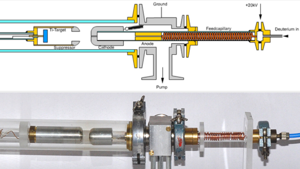
This particular generator takes a feedstock of pure deuterium, which it ionizes and accelerates into a titanium target. The first deuterium nuclei to hit the target react with it to form titanium deuteride, immobilizing them until more ions strike them and they undergo nuclear fusion. The fusion reaction mostly forms helium-4, but sometimes forms helium-3 and a free neutron, which is radiated away. The radiated neutrons are slowed down by a block of high-density polyethylene, and a portion of them strike a silver or indium foil wrapped around a Geiger counter tube. The neutrons activate the silver or indium, and the Geiger counter detects the resultant increase in radioactivity.
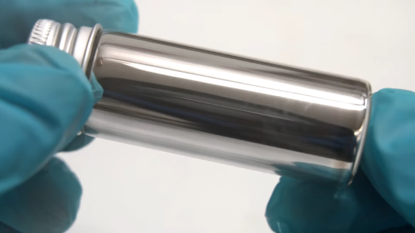
The design is a linear particle accelerator built inside an evacuated glass tube. It uses two high-voltage power supplies: a 20 kV supply which ionizes the deuterium gas fed into the tube, and a 100 kV supply which accelerates ions emitted from the source into the target. The target itself is surrounded by a cup-shaped electrode to capture secondary electrons emitted during impact. To prevent arcing, the tube needs to be at a very low pressure, reached by extensive use of an oil diffusion pump.
Radioactivity measurements of the silver and indium foils showed that the generator did work; when irradiating the silver foil for five minutes, it generated 175 counts per second after the neutron source was turned off. Plotting the count rate versus time suggested that a mixture of two silver isotopes was being generated, Ag-110 and Ag-108, based on their half-lives. Irradiation of indium produced a similar exponential decay in radiation.
We recommend checking out the rest of the site; it’s a gold mine of projects, such as this mass spectrometer. For more background on neutron generators, we’ve covered their theory and some of the more common varieties.