So you’ve finished your project. You’ve got a wonderful circuit, a beautiful PCB, and everything works perfectly. You’re done right? Well, maybe not. Sure, a bare PCB might be fine for a dev board, but what if you have a LCD to mount, a knob that needs turning, and buttons that need pressing. Yeah, that potentiometer hanging off the board by a few wires isn’t so pretty, is it? So it’s time for a case. Yuck. We all hate modifying cases.
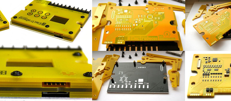
[Electrodacus] came up with a clever solution in the form of stacking PCBs to form a case. In his project, he actually has the circuitry spread across 3 PCBs, and uses surface mount connectors to connect them in a stack. Along the edges are specifically shaped PCBs to complete the enclosure. This technique could be used with only one PCB containing all the circuitry, and the others acting as the case sides and top.
In this solar battery management project, the base layer has most of the power circuitry. This layer uses an aluminum metal core PCB for heat dissipation. The center layer is home for the micro controller and supporting components. And the top layer is the “front panel” with capacitive touch buttons and a cut out for a LCD. The top layer silk screen contains the logo, button markings, and the pin out of all the connectors.
If you hate drilling and filling cases (as much as we do), this technique might be right for your next project.
[via EEVBlog Forums]


That is amazing and the link has some great pictures and models as well!
Kind of silly to use aluminium core for heat management but not having that as the outer most layer e.g. the back side.
Read the article you judgemental twat:
Make a cool case out of PCB onlyBack
Make a cool case out of PCB only by electrodacus on 25 Feb, 2015 14:17
I decided to share my Solar BMS case design made exclusively from PCB’s only.
Most are FR4 except for the PCB at the bottom that is a metal core PCB.
“you judgemental twat”: Pot, meet kettle.
The only change I’d made, is using countersunk screws. Aesthetics: 10
How well does FR4 countersink / how long of a life would your countersinks have when they are countersinking abrasive glass?
This is a good question.
Depending on the thickness of the FR4 and the depth at which one countersinks (and to a degree about over torque), one might also have to worry about stress cracking.
Maybe countersink, then seal it up with epoxy before assembly? Or some other kind of glue…gotta be something that will work.
But then you couldn’t take it apart :(
Thanks, I will actualy use countersunk screws on my next version you can see some 3D renderings on my website.
The front panel will be 2.5mm FR4 so no problem to do that.
This has been done for years, we used to use copper clad boards soldered at edges to make boxes as well. but the stacking trick was done a lot in the 80’s There was a system from brunswick that had “cartridges” that the case was a sandwich of boards riveted together.
Oh yeah. One thing I dislike more than modifying cases (which I really don’t mind, if I want an enclosure) is cutting PCB material into special shapes to form an enclosure. Its hard on my tools, creates a lot of hazardous dust, and is time consuming. With typical PCB material being 0.062″ (IIRC) thick, it will take quite a few layers to enclose components with any kind of height. Yes, this looks great if you have your PCBs made for you and you are using surface mount devices. For one-off projects and using through-hole components, this approach could cost much more than just using a case. I’ve seen amateur radio home brewers build enclosures using PCB material (see http://qrpbuilder.com/downloads/pcb_chassis_a.pdf), which looks pretty good and appears to be a lot less effort.
I agree. For most of us, spacer layers would be easier to make from plastic. Which could be printed, or cut. For cutting, Sintra (foam-core PVC) is particularly easy to work with. Unless you have access to a waterjet cutter, in which case there’s no downside to cutting PCB material; I suspect that’s the case here.
I’ve built enclosures using the technique at the link you provided. Works great for small projects. But there’s still some extra PCB cutting involved, so for larger enclosures I find myself using other techniques.
Unsurprisingly, PCB board cuts rather well overall on a waterjet. But neither PCBs nor waterjet time are considered inexpensive.
I think I’m going to have to steal this idea. Yoink.
I’m reasonably sure its not stealing if you say “Yoink”
Ctrl + C = “Yoink”
Ctrl + V = “Splat”
You are welcome :). I encurage anyone to steal the idea.
The best part of this is the ability to include a keypad as part of the lid… never buy another switch or button again… just capacitance sensors. I love this. I have a project that was stalled because of the enclosure.
Yes capacitive sensors are great and only needed a few capacitors and resistors on the STM32F072 for this.
Because of the touch keypads being the reason, it’s cool.
But SMD screw terminal without stress relieving? Is this safe?
The screw terminals appear to have a layer of PCB underneath, preventing downwards motion. Lifting force would tend to make the terminal block lift unevenly from the outer edge (ie rotate), which acting as a lever could delaminate traces. But the upper PCB cutout has such a small and gap that rotation should make the block should strike it, acting a moderate strain relief. I could be wrong, but it looks pretty solid.
I watched parts of his video, he did glue the terminal block on the board, interestingly there aren’t so many smd terminal blocks available, like what, he said about the “90 deg” smd pin-header.
Very nice work.
Speaking of EEVBlog, that site’s host Dave Jones has also done this style before, I think his video on his uCalc project (EEVBlog #130) goes into some of the design details of an example.
A related technique that Dave Jones also advocates often is combining a pre-made enclosure for 5 of the 6 sides of the case, with a PCB front panel closing it off (e.g. his uCurrent project). I think his uWatch calculator (EEVBlog #11) combines both approaches, a stack of PCBs self-containing most of the electronics, laid over top of a small plastic enclosure.
That said, this custom case is much more of a 3-dimensional exercise than any of Dave Jones’ projects, and the mechanical aspects of the design seem more detailed, which is very cool to see.
Thanks for the links to Dave. I will actually read these.
This is a beautiful project… it was on kickstarter last year. An hour long teardown and description video here: https://www.youtube.com/watch?v=_QlPJbhoiBo
$9,832
pledged of $8,000 goal
So the author basically did all of this for free and / or paid to do it?
You are right but is a hobby.
Hoping to get a bit more this time with the new version. The case has similar construction but more complex more of a 3D puzzle.
ESD!
Nothing beats a metal enclosure.
What protects touch cap sensing inputs?
Zap!
Keeps RFI on the inside as well. Keeps hum out.
There’s plenty of effective ESD protection.
Also, have you ever tried to zap the cap inputs on things? I use AVR GPIO with a ~1mohm pullup and I’ve felt an arc go from my finger into the pad and it doesn’t seem to even notice.
Awesome pics. This seems like a great project and they did some good work on it.
Someone has been watching mikeselectricstuff.
Interesting concept… And with cheap PCB fabs these days, could make things quite easy for those (like me) that don’t have easy/cheap-access to other forms of CNC-cutters.
But, aren’t most PCBs fiberglass? Don’t think I like the idea of little shards of glass being on the edges of my enclosure.
This guy is doing some nice work I can’t wait to tinker with these
oh yea his v2 is on the kickstarter
Well, this just gave me idea to make suitable DIN rail enclosure from FR4 board bcs i’m searching for some box long time ago to put my “PLC” in it… :) thnx @electrodacus