Are you the kind of hacker who tries to pick up FreeCAD, but doesn’t want to go through a tutorial and instead pokes around the interface, trying to transfer the skills from a CAD suite you’ve been using before? I’ve been there too, and in my experience, FreeCAD doesn’t treat such forays lightly. It’s a huge package that enables everything from architecture to robotics design, so if you just want a 3D-printed case for a PCB project, the hill can be steep. So let’s take that first simple project as an example, and see if it helps you learn a little bit of FreeCAD.
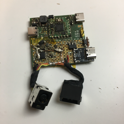
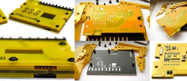
As motivation, I recently built a USB-C PSU board that uses a DC PSU and does the USB-C handshaking to provide 20 V to a laptop. It is currently my only 100 W USB-C PSU, and my 60 W PSU just died, which is why I now use this board 24/7. I have brought it on two different conferences so far, which has highlighted a problem – it’s a board with tons of exposed contacts, which means that it isn’t perfectly travel-friendly, and neither it is airport-friendly – not that I won’t try and bring it anyway. So, currently, I have to watch that nothing shorts out – given the board has 3.3 V close to 20 V at 9 A, it’s a bit of a worry.
This means I have to design some sort of case for it. I was taught SolidWorks in the half a year that I spent in a university, and honestly, I’m tired of the licensing and proprietary format stuff. When it comes to more hobbyist-accepted tools like Fusion360, I just don’t feel like exchanging one proprietary software for another. So, FreeCAD is the obvious choice – apart from OpenSCAD, which I know and love, but I don’t always want to think up fifteen variable names for every silly little feature. That, and I also want to fillet corners every now and then.
For a full-open-source workflow, today’s PCB is designed with KiCad, too. Let’s see about installing FreeCAD, and the few things you need to import a KiCad board file into FreeCAD.