It’s no secret the Hackaday tip line gets a lot of email from Kickstarter campaigns and PR firms managing Kickstarter campaigns. Most of these are terrible products. Want a five-pound battery that can’t be recharged? Yeah, stuff like that.
Every once in a while, we come across a tip that’s a completely original idea. There’s a balance between ingenuity and practicality with these ideas, and I can’t figure out where this one sits. It’s a Kickstarter for perfboard, yes, but not like any perfboard you’ve ever seen.

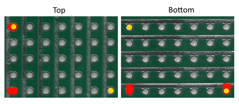
Before we dig into this, let’s get some definitions straight. Perfboard is a sheet with holes drilled on a 0.1″ grid. The holes are plated on both sides, and each hole is an individual electrical node. Veroboard, or stripboard is a bunch of holes on a 0.1″ grid. These holes are also plated, but all the holes in a column are a single electrical node. You can cut the tracks between holes, but the basic idea here is to reduce the number of wires needed to connect components. Busboard, seen left, is a continuation of Veroboard, and is laid out like a solderless breadboard.
And so we come to the new invention, Perf+, the perfboard reinvented. This perfboard again is a series of plated holes on a 0.1″ grid. Alongside these holes is a plated bus. This bus does not connect to any hole; instead, a little bit of solder is used to connect it to holes on the same row or column. “Selective Veroboard,” you could call it.
Now for the real trick: on one side of the board, the plated busses run vertically. On the other side of the board, the plated busses run horizontally. This means any two holes on the protoboard can be connected as one electrical node simply with a bit of solder.
If ever there was an idea you could point to and simultaneously say, “that’s clever” and “I have no idea how to use this,” there you go. I’m pretty sure this idea isn’t better than a piece of stripboard, but it is different. If you have any idea of how to used this new, strange, and otherworldly protoboard for something useful, put a note in the comments.


So… If I understand correctly… Every Via is connected?
So the idea must be taking away, rather than adding.
They must expect you to cut away the pathways you want to use?
Seems that you can connect a hole to an bus with solder.
They don’t come already connected.
They look connected, but if you look really really close, it seems they’re not.
What’s bad about this is the fact that there is hardly any clearance. If those are standard sized holes, the break between the via and bus is on the order of 500um. It’s going to be extremely difficult to not accidently solder the via to the bus. So in my opinion, if this was the intent of design, it is a total failure.
They state the gap is 8 mils.
looks like it would be good for leds or cap banks but thats about all
yep. no practical use. as soon as you connect one thing like they show on their page, now your entire left and bottom row of hole become a useless wire.
this thing just recreate all the problems the protoboard layout solved over the decades. but they are going to learn *after* production. sigh.
just, no.
breadboard layout i meant.
It’s very simple (and interesting). On one side there are strips connecting the holes horizontally, but not through hole to the other side obviously. And on the other side the same but rotated 90 degrees so you have a vero board that actually has dual layer functionality but for experiments.
The question is though if you should have every line like that, it might be better to have one side have it on every row of holes and the other side 90 degrees but strips for every third hole (that’s the spacing of standard 4 pin chips right?) for instance, rather than also for every line of holes. Because obviously one side will have the components and then it becomes inconvenient to have to scratch a large number of connections.
404 error on the link. Must have been dreaming
Correct link is:
https://www.kickstarter.com/projects/658903329/perf-the-perfboard-reinvented?ref=nav_search
https://www.kickstarter.com/projects/658903329/perf-the-perfboard-reinvented
The problem is that PTH pads make it a nightmare to desolder anything, which is crucial for a (duh) prototyping board…
That’s what breadboards for!
Yes indeed, well said. Who the hell desolders a whole vero board? Although you might occasionally desolder a single part to correct something, but that should be doable with some desoldering braid and by pushing while it’s hot.
Maybe so but you will probably have mistakes to fix and this will make it difficult.
Decent tools make desoldering and rework much less painful.
AKA “Nearly Invisible Accidental Solder Bridge Board”
This ^
Good luck trying to fix any mistakes with a tiny bus bridge gap like that. Unsoldering anything won’t be fun as well with plated-through holes.
It is a nice idea though and it’ll stop the bad practice of just globbing loads of solder everywhere to form traces.
The holes aren’t plated through, although of course when you have a part going through and then apply solder it becomes so. But at the point you use vero board you should already have the design tested and it’s just about avoiding making a whole custom PCB for a single instance.
It’s fascinating to see several people here who apparently use vero board like you use breadboards and they solder a whole project then desolder it again. Amazing and weird stuff.
Suppose I should chime in, as someone who pretty much never uses breadboards since circuit courses as an undergrad (for EE)…for a huge realm of circuits, even if you have through-hole parts…you either know it will work or not (like digital stuff, for which now if you’re really not sure your combo-logic or state machine will work, you just simulate it) or it’s analog stuff that you don’t know will work, which is often in the realm of stuff that really doesn’t like the huge distributed capacitance and highly resistive connections of breadboards. I honestly think it’s often faster just to solder everything, and then I don’t have to do it all over again if it falls off my desk…and I can stick it in a box of things, and if I need to come back and look at it in a month (or year), it’ll still be as it was.
Then again, there is a huge gulf in quality between cheap and not-so-cheap breadboards, and the nicer ones can really save headaches when it comes to reliability.
But would you desolder the whole thing? You say you throw it in a box not that you do such a drastic design change that you need to many several parts.
In my experience when I use a vero board I designed it first on paper (sometimes literally paper) and it’s suppose to work, and I don’t recall desoldering the whole thing. But I have to add that I tend to use sockets for chips if it’s at all possible, so that if I fry one it’s an easy replacement.
Correction: “need to desolder many parts*
Bad practice? With practice, you can make some gorgeous boards (with fantastic analog or power performance) that way!
I want one right now. :)
I am hacking a 2 gig sd card onto a linksys wap54 router to use for stuff.
This seems like a great idea and lot cleaner then a breadboard filled with wires.
I’d be more interested if there was some autorouting software to go with it.
Never trust the bloody auto router!
AMEN!
I was thinking the same thing. While Veroboard looks simple enough to do a layout, with this it would need some planning to get the parts laid out properly.
should be possible to accomplish this using eaglecad
I have an auto router that routs the top and bottom conductors at 90 deg to each other. It is part of Visionics’ EdwinXP.
This looks like a royal PITA to use – very easy to make inadvertent shorts where you don’t want them, with the distance to the bus so narrow. Also the annular rings look awfully thin – bad idea for a protoboard, they will be peeling off real quick. The idea is neat, I hate having to solder tons of point-to-point jumpers on perfboards, but the execution is poor, IMO.
I clicked report on accident… Sorry about that.
http://kck.st/1J3YTVh
“If ever there was an idea you could point to and simultaneously say, ‘that’s clever’ and ‘I have no idea how to use this,’ there you go.”
That may be the most perfect summary ever.
But aside from how to use it, it seems like this has a more serious flaw. I can barely see the gap between the busses and adjacent holes. Seems like it would be hard to avoid inadvertent solder bridges, or find them when made. Looks like a HASL finish, so your board might even come with a few nearly-invisible bridges straight from the Chinese board fab. And I’m no expert on tin whiskers, but isn’t one factor in their growth charge differentials across tiny gaps exactly like these?
The final product will have a ENGI finish so there should be no solder bridges out of factory.
If you want a matrix of led, this is probably the best protoboard, but for anything else, it will be very easy to made a magic fume circuit :)
button matrix too maybe
that’s actually genius as you can, as the trace seems fine enough for doing this, cut the track as well as link pads to it (even if a wider gap would be easier to manage)
that means you are able to jump over other tracks without jumper wire and to reach areas of the board with a particular signal or voltage reference without resorting to CAT5 wire or other easily melt wires…
this is also a nice trick for playing with SMD as you would be able, if the gap between a row and a pad was a bit wider, to have even pins of your IC to one face of the board and uneven pins on the other, which would permit clever routing tricks and circumvent the problem of having just 4 pads to the one you need with small busboard, for instance, as you could basically play tron with your signal
I foresee that to be a revolution in protoboard, if you think out of the box
I’m struggling to understand why folk are having issues getting their head round this.
Sure it adds a level of complexity to a prototype, but it can be utilised to an advantage. Admittedly, you will have to make twice as many cuts, but if it fits your application, then your work is halved nearly!
I think it’d be more useful if the bus weren’t tinned, and there was a larger gap between the holes and the bus. My problem with the bus being tinned is that it makes it harder to cut it apart. I think they should only remove the solder mask on the bus right above the hole. That way you have islands between the holes that can be easily cut.
This looks like a really neat product, but I don’t expect it will become terribly popular.
This looks potentially ingenious if you can handle the co-planar routing in your head. But, I wouldn’t trust that every through hole is indeed disconnected and would end up toning everything. BUT, as a semi-permanent board for a prototype that has to be somewhat robust, I might try it.
Perf+ is being renamed after its inventor. It is now known as a Wangboard.
here’s an idea – anyone ever seen this before? make the cuttable sections electrically fusable. meaning, you use probes that fit into the hole/pads and those burn the trace between them. the trick is how to do all of that (lots of details). but that’s the overview. cutting with a knife is so barbaric. there should be a way to have geometry work so that the link between 2 pads can be broken reliably and cleanly. bonus points if you can solder rebridge the fused/blown sections, at least once more.
That’s a neat idea, but it would be tricky, you would need to blow the links before attaching any of your parts to the board, so some careful layout planning would be required. The links themselves would need to be pretty small, but a quick capacitor discharge could blow one without burning up to much of the board.
I do like the idea of having narrower points where you could cut the traces more reliably.. and also re-bridge them if need-be. Maybe you should suggest said idea to the creator, I would think it would make an improvement to the design by far.
Take a look at the update. Not sure if it came after this comment or not, but he is planning a pretty neat modification.
Yay! We can all change the world if complain enough on the internet. What a great time to be alive!
I tried that with a regular board I etched to blow out a short, and blew out two inches of traces. 55VDC at nearly unlimited current is really not a good way to go about that.
I do think there is potential for fusable boards though.
No, there is no potential. When FR-4 burns and carbonizes it becomes conductive (at least across small distances/thicknesses). Been there, done that.
If the many megaohms of resistance is too low for your application you shouldn’t be building it on perfboard anyway.
Clever, sure. Now show me a completed circuit I’d use made with this stuff.
I’d like to try this out. I don’t know whether I’ll prefer it over regular perf, but I definitely think it is worth a shot.
It is the sort of board Harry Potter would use, align components Diagon Alley.
Don’t tin the traces but align traces exactly in the middle between two rows of holes. Then make very small copper islands in the middle of four holes. Then use a bread/bus-board like layout (sections without traces) and i would be very tempted to give it a try.
I agree. That would be way more useful.
Or don’t put the traces there at all, and you can just run 30 AWG wire between pins you want to connect. You know, like on perfboard. Seriously. I don’t see any advantage, just like I didn’t with Veroboard, after trying to use it a couple of times.
Here’s my money. Now please make some boards with commonly used pads, dil, soic etc but no holes for us old farts who love dead bug or manhattan style construction. Thankyou.
I don’t want to spam or anything, but you may like my approach to this; see https://www.tindie.com/products/Springuin/opamp-prototype-board/ for pictures. It’s design is opensource: https://github.com/Springuin-nl/OpampProtoboard
That’s a nice board. i like it.
take a look to my design, its combining PTH and (almost) SMD can fit. i designed that about 3 month ago. Double layer non through hole so you can wiring on both side. https://hackaday.io/project/3859-zuc-protoboard
I have the same comment as someone else had for the product this article is about: show me a picture of a practical circuit using this.
Done:
https://www.kickstarter.com/projects/172605143/zuc-proto-board
Isn’t this “one side horizontal, one side vertical” scheme basically what was used in the 80’s to route double sided PCBs?
Yeah. Every old computer used something like this. For perfboard, though….
It is still used by Visionics standard autorouter in their Edwin pcb software. It looks like I could layout the circuit with the autorouter and put it right onto the breadboard.
At first it looks like a neat idea. But then how do you solder a 805 SMT resistor or capacitor between adjacent pads?
I’ve backed this one because I think it’s an interesting and useful concept but I can see some potential problems, particularly with DIP ICs. What I want to see is if soldering a pin results in an inadvertent bridge on the “top” side of the board i.e. the side holding the component. If it does then that means you’d have to drill out all holes for IC pins on the top side so that neighbouring pins don’t wind up connected to the same top trace. Could probably be solved in a future version with a few dedicated IC pads scattered around the board?
If one does not use massive amounts of solder, it is practically impossible to bridge the “bottom” side while soldering on the “top” side.
Thanks for the clarification, and congrats on the successful campaign. Looking forward to making something with them.
There’s a HUGE problem with the idea.
Imagine placing an IC on the grid, and needing to route more than two adjacent pins to some location. Any way you place the chip, you’re going to have all the pins align to the same bus strip. From a practical point of view, this is no better than a veroboard.
Exactly
If you solder one side, the other side does not bridge over, allowing you to use ICs easily on this board.
See: http://imgur.com/4cUR9AV
where yellow is the signal broken out, red is solder and black is where you cut the traces.
That’s not what I meant.
Each pin has a separate bus on one side of the board, but a single bus for all the pins on the other. If you need to connect multiple pins of an IC, the system is practically useless because they’d have to share the same bus wire.
Very quickly it turns into a connections puzzle, because you have to spend time figuring out how to route your signals around the edges and how to approach particular pins, and by that point you’ll just cut a jumper wire and do it the simple way.
The busses are not connected by default to the pads, you need to place a bit of solder to connect it. ICs won’t get shorted out.
I agree with some of the other comments, ENIG rather than HASL it, make the gaps a bit larger, and increase the annular ring so you don’t have to be paranoid about bad connections. Then it would be something I’m interested in giving a shot.
Also, maybe silkscreen on one side where the traces are on the other side?
It is so much easier to just lay down copper wire and solder the holes. I would rather add then cutting.
Sadly, the best proto boards I am buying are from china. $0.10 to $1.00 each and are fantastic! Better than the stuff from the big parts houses or smaller ones like sparkfun.
Looks like just the thing for custom keyboard builds.
As it’s really easy to scrape off solder-mask, I’d cover the buss lines with solder-mask to avoid unintentional connections. I’ve also thought it would be nice if there was perf-board with a solder-masked, isolated net between the holes on the top and bottom. Used as power and ground, these nets would eliminate about half the routing in any circuit. The nets would also function as a ground-plane so circuits would work well at high frequency.
This already exists, We have a huge stack of it at work but nobody uses it because it is annoying to work with. It looked quite old when I had it in my hands last time so the idea is certainly not new
Photo to compare to this “new” version?
Not at work due to obvious reasons, but I’ll see what I can do in a few days when I have to appear at work.
I agree with the spacing being too small, but how about increasing the distance and giving a small wire solder point on the other side of the via? Not everything you do is going to work on a linear track. With the ability to jump to an entirely different place on the board you can make this (with the gap adjustment previously mentioned) into a decent mid level prototyping board.
Of course, after seeing this, I want to mill out a version on my CNC to test out my idea for improvement.
Would be better if the pattern is similar to a Veroboard, but with traces underneath perpendicular to the vertical strips. I kinda like how the veroboard works, and this would greatly reduce the jumper wires needed. (except when linking strips on either side of the middle power rail.
Great board, backed 8-) Imagine that crossed with this one https://www.indiegogo.com/projects/proto-e-surface-and-through-development-board wonder what would offspring look like!?
[youtube http://www.youtube.com/watch?v=AcyHT7Q7tDo&w=560&h=315%5D
Im not really buying it, i mean, when one pin is connected to a row, the whole row is waisted, and theres no way to conntect to another rowexcept with jumper wires… so the whole purpose is kind of gone.
wouldnt be patterns like this (sorry its just a quick sketch) be better?
https://dl.dropboxusercontent.com/u/1484680/hackaday/pattern1.png
https://dl.dropboxusercontent.com/u/1484680/hackaday/pattern2.png
(on the backside same pattern but rotated 90 degrees)
I think the point is you can cut the trace to break the row into multiple sections. To connect to a non-adjacent trace you would use through-hole and connect to the perpendicular traces, then back through at the other connection. Again cutting the traces in the directions away from where you are actively using the trace, allowing you to use them for other routing.
right… auto-router-style perfboard. I dig it. It could definitely stand to go through a few design-iterations, but if it never gets the chance then… it won’t get the chance to improve.
I’m a little confused why no one seemed to point out the most obvious of all obvious-factors… how is one to bridge those joints on the top-side when the chip/resistor/whatever is physically covering the bridge-point?
Also, so many comments on the annular-ring-size… I’m a bit confused, is this through-hole-plated or not? If it is, does the annular-ring *really* matter in a case where there’s not a trace coming out?
And, dude who suggested that desoldering THP is difficult, get a (good) solder-sucker, there can’t be anything easier.
As it stands, could be useful for certain tasks, for sure. If nothing else, just use the top busses for V+ and the bottom for GND, saves a *lot* of work, as someone else suggested… And with the option to *not* use them all that way.
Dax brought up that problem above. That’s why it would be better if the traces were centered between holes. They are plated through holes, so the annular ring doesn’t really matter.
I remember doing something similar, putting two veroboards back to back, turned 90 degrees apart. Looked very neat.
Now I just drag those Teflon insulated wires from point to point.
I love everything about this idea! Except maybe the gaps are too narrow. We’ll see how it works in practice. The ENIG plating and choice of solder will make or break it.
Figuring out the wire routing and optimal component placement on a perfboard is something I find incredibly pleasing, even if it’s time-consuming. Turning the board over in my hands, looking back and forth between datasheets and schematics and actual component packages, trying to arrange something so all the hot parts get heatsinks, all the sensitive signals are away from the high-power signals, and there’s a minimum of wire on the board, just seems to exercise some part of the brain I really enjoy.
Backed the project. I can’t wait to try my hand at this stuff!
It hurts my head to imagine an analog circuit with 10+ components on this kind of board. The mental overhead to organise the traces isn’t worth it, IMHO. But the idea is intriguing. I’m just to dumb to plan such a circuit. I would rather use a wiring pen and enamel wire.
Actually make the gap 10 microns instead of 8 and I can use it as if it was a prototype board I designed.
By the way this is perfect for the Adafruit breadboard fritzing libraries. Design it out then solder the junction holes.
Whatever happened to the Atarado boards? http://www.atarado.com/index.html
+20dBm Typ. (+30dBm Survival) Frequency Variety 1.75:1 Max.
For me is a NO-NO..!
How one ca put a standard DIL there without shorting pins?
Every point is isolated from each track and you only join the ones you want but its very difficult to see from the image,you could use any IC and drastically reduce the use for any wiring
Obviously there would still be some cuts and wiring that need doing but its still a lot easier than point to point wiring everything
Any 2 terminals on the board can be bridged by soldering a couple of simple joins to the corresponding tracks on the grid its quite brilliant,it almost completely eliminates the need for any wire or cutting of tracks at all.my only concern is how close the bridges appear to be between each terminal and its corresponding track but it probably looks a lot better in real life,if it works fine in practice then i’m sold
I have ordered 5 of these, however I cannot figure how to download the ‘Perfy’ software from Github.
For anyone else that sees this go into binaries -> Perfy-1.0.0.3.zip and click on the “Raw” button.
Nevermind, just getting blind in my dotage, heh.
Maybe inspired on Crossbar switch would have potential for prototyping or test internal PROCESSOR BUS DESIGN, MEMORY ARRAY, MEMS… Is practical for solder in one side Active components (mcu, processor, memory, clock,) and on the other side pasive components (resistors, capacitos…) for and elegant presentation of this kind of design.
In real world this perfboard seams to have non conventional application, but is how Internal chips MCU and Processors are interconected!
Here give some research and images about potential uses.
https://upload.wikimedia.org/wikipedia/en/7/76/Crossbar-banjo2-hy.jpg
https://upload.wikimedia.org/wikipedia/commons/2/21/Single_bus_organization.jpg
https://upload.wikimedia.org/wikipedia/commons/thumb/4/42/80486DX2_arch.svg/2000px-80486DX2_arch.svg.png
https://upload.wikimedia.org/wikipedia/commons/thumb/1/1c/SMP_-_Symmetric_Multiprocessor_System.svg/1280px-SMP_-_Symmetric_Multiprocessor_System.svg.png
A 6502 computer https://imgur.com/a/nQGwa
A 3D printer controller with SD card slot and WiFi https://imgur.com/a/U2wIz