
[Ralph Doncaster], aka Nerdralph, seems to be absolutely driven to see how few resources he can use on a microcontroller to get the job done. In this post on his blog, [Ralph] writes some custom bit-banged SPI code to cut the number of SPI lines necessary to drive an nRF24L01+ radio module from four down to two. That really helps if you’re using a micro with only six free pins, like an ATtiny85.
If you’re going to say, “why don’t you just buy a bigger microcontroller?”, you’re missing the point. This exercise strikes us as optimization for optimization’s sake and a dirty hack, both of which are points in its favor. There are also a couple of techniques here for your mental toolbox. We thought it was interesting enough to look at in depth.
Before we dive in, here’s what you’ll need to know about SPI in three sentences. SPI normally uses four wires for a simple master/slave setup. The master sets a chip-select line (CS) to let the slave know it’s being spoken to, and starts toggling the clock line (SCK). Two more lines are used to carry data from the master to slave (master-out-slave-in or MOSI for short) and from slave to master (MISO). So how does [Ralph] combine these four into two?
Trick One
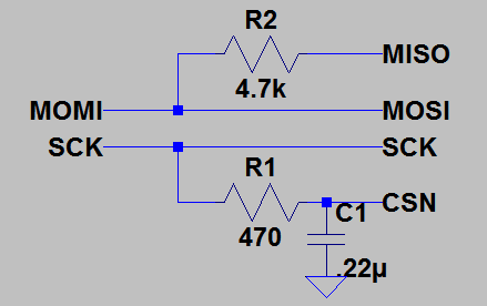 To merge the clock and chip-select lines, [Ralph]’s circuit relies on a modification of a trick that he’s previously used. Notice that the CSN line on the radio module is connected to SCK on the microcontroller through a resistor and capacitor to ground: through a lowpass filter. With the values set just right (which will depend on the clock frequency) the value on CSN will be the average voltage on the SCK line, just like when you use a lowpass filter to smooth out “analog” PWM output.
If the clock uses a pulse-width narrow enough to average to a logic low when the clock is running, the CSN line will get pulled to some in-between voltage that’s low enough to be interpreted as logic low when the clock ticks, and the nRF24L01+ will start listening. [Ralph]’s custom SPI code uses a 25% duty cycle to make this work.
When the microcontroller is done sending clock ticks, it will hold the clock line high for a relatively long time, pulling the CSN line high, and letting the nRF24L01+ know that it’s no longer being spoken to.
Trick Two
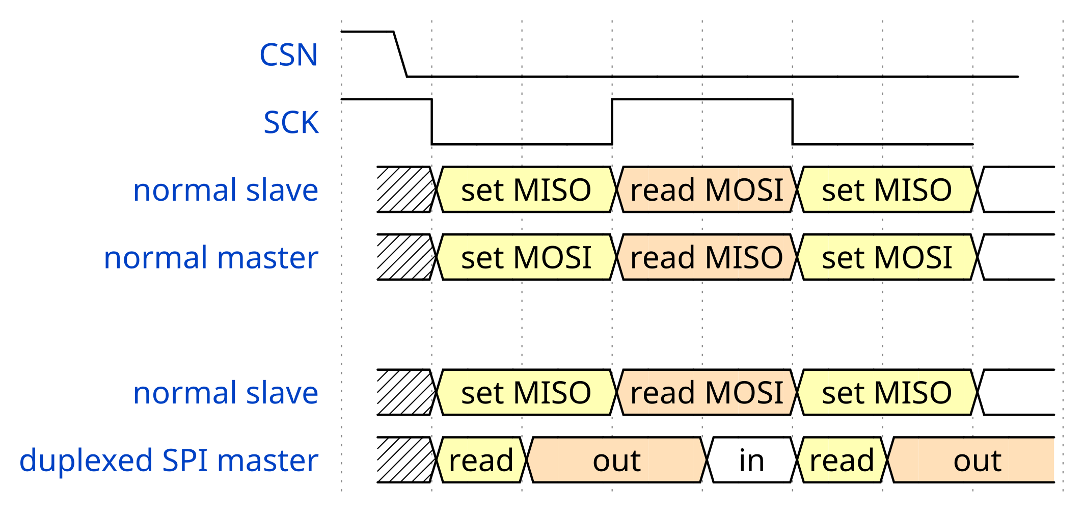 Now let’s look at the hack to multiplex MISO and MOSI into “MOMI”.
Normally, both the master and slave set up their next data bit on their respective output lines at the same time, after a low clock transition in this example. Then both parties read their input lines after they see the clock line flip high again.
In [Ralph]’s duplexing scheme, the master sneaks both a read and a write to the single “MOMI” line within the setup period. (Note that we used a symmetric clock in the graphic above, rather than the 25% duty cycle that [Ralph] needs for the chip select hack.)
When the clock transitions low, the nRF24L01+ starts to set its desired output voltage on its MISO line, which is then read by the microcontroller. While still in this setup period, the micro then switches to output mode and establishes its desired voltage on the line before it toggles the clock high again, signalling the nRF24L01+ to read from the line. The master then switches the pin back to input, allowing the nRF24L01+ to control the line, but doesn’t read yet. Finally, the micro drops the clock to repeat the cycle for the next bit.
There are two things [Ralph] needs to get right to make this duplexing work, and the first is the timing. On a low clock transition, the nRF24L01+ sets its output voltage. A little bit of time has to elapse until the microcontroller can reliably read this voltage, and that time will depend on the line’s capacitance, the value of resistor R2, and the strength of the nRF24L01+’s output driver.
Then, after the microcontroller has read the nRF24L01+’s voltage, it will impose its own output voltage on the line and then toggle the clock high again, signalling the nRF24L01+ to read the value. Here, R2 needs to be chosen large enough that it allows the microcontroller to override the nRF24L01+’s own MISO signal.
So picking the resistor R2 is key. It has to be selected small enough that the nRF24L01+ can set up its desired voltage on the shared line before the microcontroller reads it in. But the resistor also has to be large enough that the microcontroller can easily override the nRF24L01+’s own output coming in through MISO. [Ralph] used an oscilloscope to pick the right R2 value, and it works.
Conclusion
But that’s probably also why this type of arrangement isn’t seen much in the wild. Engineers love simple protocols that work reliably across different circuit layouts and with added noise. Here, [Ralph] is using a low-but-not-digital signal level for CSN and then hand-picking a resistor based on line capacitance and the nRF24L01+’s output driver strength, which is not something that Nordic specs for in making the chips. In other words, be prepared to tweak the value of R2 or play with the SPI timings if you try this at home.
In sum, though, this is a sweet hack — an attempt to get the most out of a constrained system by hand-tweaking it beyond the point that any reasonable engineer would. We like that. But by doing so, is [Ralph] living on the edge? Or is the entire system more robust than our inner engineer gives it credit? What are your thoughts, and if you try it out, your experience?
Embed with Elliot is a column in which microcontroller expert [Elliot Williams] explores and explains interesting, clever, unique, strange, and sometimes wrong uses of embedded systems. Help keep this column fresh by sending in tips for the next installment.


Actually, in ultra high volume electronics you see similar crazy stuff all the time. Saving on BOM can make a huge difference. When I was first out of school we did TV repair in college. They did all sorts of wacky stuff with transistor circuit design to save parts. The output design here is pretty usable. The input scares me. :)
Not all SPI slaves allow merging data lines. Read target specs carefully before trying.
I’m sure that’s true, but it kinda makes SPI as a bus pretty useless.
It seems like you could add transistor buffers to MISO and CSN to eliminate issues with variability on the SPI interface.
Sure, I’ve seen this, and approve if there’s a good reason for doing so (with a good reason being whatever the designer considers one). A few comments:
1) You CANNOT access the full functionality of the NRF24L01+ with this circuit and only two pins! To switch the NRF from receive to transmit (and back), you need to pulse another pin low (CE). It’s not documented in the datasheet, but you’ll also need to pulse CE low to reliably change channel more than about 100mhz from the previous frequency, else the PLL won’t lock properly (at least on the fake NRFs, which seem to vastly outnumber the real ones at this point, so might as well design to accommodate either). And you can’t detect interrupts from the NRF, though that’s optional if it’s acceptable to poll the device.
2) I’d feel more comfortable changing R1 to a pull-up, and having SCLK pull the RC circuit low through a small-signal diode. Would make the CSN signal more robust if SCLK isn’t a 1:1 duty cycle, repeated interrupts occur during bit-banged transfers, etc.
3) This won’t work if you have multiple devices on the SPI bus, which is often when you need to conserve pins.
Actually you can switch Rx/Tx, you just have to switch to power down mode first. I explain this in the comment thread of my original 3-pin nRF control circuit.
Aha, that’s clever! And since that causes the PLL to reset, it also solves the issue with changing channels. IIRC there’s an additional delay for the NRF to come out of power-down mode, but that won’t be an issue for many apps.
Yeah, this kind of stuff is used all the time in high volume electronics. I took a job interview with Apple some years back… definitely with the wrong part of the company. These guys were less concerned with the fact I had single handedly designed ARM computers with high performance discrete RF sections, written all the FPGA and low level code, filed patents on it, etc. than whether or not I knew some “stupid transistor tricks”. But when you think about it, even if Apple’s volumes get them the transistor for 25 cents that everyone else buys for 45 cents, it’s still going to save them half a million bucks or so. Do thaDave t a few times per product and you’re talkin’ some real money.
The other thing that could be consider is that bitbang SPI pins could be shared with other interfaces. When the /cs or strobe is deasserted, the SPI device ignores what’s on the I/O. There are similar sharing trick with bitbang I2C.
I would try the other tricks first before doing this. I am not a fan of slow rising edges for strobes unless you know for sure that the device has Schmitt trigger inputs and that you haven’t violated the timing rise/fall time in the datasheet.
That’s ingenious! Thanks for sharing. Even though it might not be used for all spi devices it is definitely a good trick to carry in the pocket.
Excellent article Elliot! The timing diagrams and details on how SPI normally works explains it better than I could.
nice hack! And, of course, some SPI slaves can function with CS asserted all the time.
The use of a low-pass filter–indeed, the use of any reactive components–disqualifies this, as well as any design, as a logic design. A design such as this submitted as an RFP by a contractor would not even merit a response. A design such as this submitted by an employee would result in a serious career track slowdown.
Perhaps HAD wants to institute a new hack category: “Kind’a Analog; Kind’a Digital”?
Please respond quickly. We’re all awaiting your answer with bA/Ded breath.
Well, maybe in your little world. But in the world of Fairchild, Phillips/NXP, Motorola and Onsemi it is a perfectly fine thing to use low- and high-pass filters in logic designs to achieve pulse doublers, edge/pulse detection/stretchers/shorterners and function blocks like that.
http://www.onsemi.com/pub_link/Collateral/AND8408-D.PDF
Maybe they are all wrong in recommending that, and should not even merited a RF[I/Q/P] due to their abhorrent design techniques and recommendations? Hm?
You have just displayed the worst side of the term “hacker”, and your place in that spectrum. Don’t talk to me about “…little world…”. As one of the commenters points out, most all of your “valid examples” of “true” logic design are accompanied by Schmitt triggers or the like; and your “proofs” are for use in VERY ISOLATED parts of a logic system such as clocks and waveform shaping; NOT within a synchronous logic design.
You are obviously unaware of the fact that any true logic design is synchronous, and this is the precise reason why monostable multi-vibrators are never seen in a true logic design SYSTEM (except, possibly, yours).
MINIMAL experience in logic design–and common sense, hubris control, and the loss of “hacking” as the only electrical engineering design “qualification”–would be highly desirable before capability to comment on others’ design experience and suggestions is–wrongly–assumed. Oh, and a smattering of humility wouldn’t hurt, either.
Good luck, and warmest regards…
“Oh, and a smattering of humility wouldn’t hurt, either.”
Pot, meet kettle…
R. Service: Perhaps you could post a link to your expert designs.
Thanks
Props for that link… I’ve been back-burner wondering for quite some time about using a method like this for frequency-doubling. R/C filtration + XORs, DUH… (and here I was trying to use AC coupling and stuck on what to do about those negative-spikes).
Notice that *all* of the examples are only combination gates and some with schmitt triggers input that are designed for slow rise/fall time. At no where have they shown that you can do the same with D type latches where there is a maximum rise/fall time on their datasheet.
Without checking with datasheet to confirm maximum rise/fall time, it is a hack not a proper engineering design. It *might* work for you at a certain temperature/voltage for a small sample design.
The site’s name is HackADay, not BestPracticesADay.
Passive filters are often used for slew limiting on fast signal transitions for emc. I dont really understand the hostility here… Those people are never fun to work with.
Good call on both fronts. +2
I wish someone would translate Ralph’s post into something a beginner can understand. While it’s great that he’s achieved this, it’s difficult to follow his examples.
You can add a diode across R1 to avoid the need for a custom duty cycle on the clock. /CS will come within a diode drop of clock low even at less than 50% duty cycle and RC is the release time of /CS after clock remains high.